
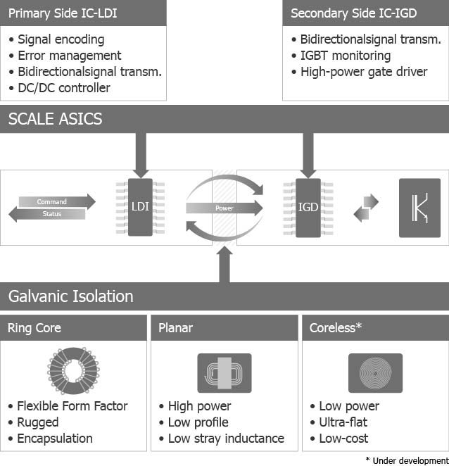
SCALE-2 ASIC 芯片组
CONCEPT SCALE™-2 IGBT驱动器利用ASIC芯片组来降低元件数量和尺寸,同时提高性能、可扩展性和可靠性。利用芯片组,设计师可优化动态切换性能、精度和功能,实现灵活的设计并缩短上市时间。
SCALE-2芯片组 – CONCEPT的IGBT和功率MOSFET门极驱动器的下一代技术 – 针对IGBT以及150A到3600A和600V到6500V的应用优化,但是也可预配置以促进应用特有的设计。ASICS在汽车级BiCMOS晶圆工艺线上制造,确保其高度可靠。
CONCEPT的第一代SCALE驱动器在世界各地被大量使用,已成为各种应用的标志。高度集成的SCALE-2门极驱动器芯片组具备所有必需的功能,可提供高达60A的门极电流及20W的驱动功率。副边ASIC集成了预驱动单元,用于驱动芯片外部扩展的N沟道DMOS,这样的推动级能够单独的设置开通和关断电阻,以独立控制开通和关断行为。
SCALE-2技术技术带来了新的产品特性,包括副方的智能门极驱动器(IGD)芯片和一个原方的双通道逻辑驱动接口(LDI)芯片。
ASIC:智能门极驱动器(IGD)
图中所示为驱动器副方ASIC的显微照片。使用不同的键合方法进行生产,以控制标准产品的特有功能,包括双向变压器接口与光纤接口的芯片。ASIC中还包含一个半定制阵列,可以用于客户定制。高级控制选项可通过单次编程的金属掩模实现。半定制阵列包含预配置的单元,例如模拟比较器、逻辑门、基本元器件和焊盘。
IGD ASIC通过调节“Vee”管脚(如图3所示)的电位,使IGBT开通和导通状态的门极-发射极电压为稳定的+15V,或者根据客户的需求定制为其他值。
ASIC可以实现在IGBT关断时,对集电极-发射极电压的上升率[1]和箝位水平[2]实现闭环控制。这样可以获得更快的有源钳位响应速度,更低的关断损耗,以及更强的短路关断能力。
ASIC:逻辑驱动接口(LDI)
图2所示为原方的逻辑驱动接口ASIC的显微照片。该ASIC包括了两个通道的双向变压器接口、具备特殊上电时序的可扩展的DC/DC电源以及故障管理模块。
CONCEPT’s SCALE-2 IGBT-drivers couple ASIC technology with a proprietary transformer design enabling the company to provide UL Certification across its entire product range.
A bidirectional transformer interface transmits both command and fault signals via short single pulses to achieve minimum command delay. In case of a signal collision, the fault signal dominates both the command signal and dv/dt induced noise currents by means of a longer pulse duration. The asynchronous fault transfer method also allows the special timing requirements of parallel-connected IGBTs or multi-level converter topologies to be managed, since any fault condition will be apparent at the primary side in less than one microsecond. A preferred fault-management mode reports the fault event in advance of a turn-off of the relevant IGBTs. The delay period before shutdown can be adjusted within the IGD ASIC. For transformer coupled drivers, (see Fig. 3) delays of less than 80ns and ±1ns jitter can be achieved.
Operational Modes
Direct Mode allows both driver channels to be independently driven. This mode offers the highest levels of customer flexibility and is therefore preferred for advanced microcontroller-assisted systems. In half-bridge mode, the ASIC uses only one input as a common command signal and generates two (non-inverted and inverted) outputs. The mode and dead time are adjustable to the needs of the particular application via a single resistor. A third mode is pre-configured to implement interlock or mutual exclusion upon customer request.
Fault Management
On the primary side, any fault state may be stretched by a Blocking Time. During this period, the relevant channel is kept in the off-state. This time is adjustable using a single resistor and can also be set to a minimum of 10μs.
System Integration
CONCEPT's proprietary SCALE-2 chipset serves as a core technology for implementing the next generation of IGBT driver series. Fig. 4 shows a simplified schematic diagram of a Plug-and-Play IGBT driver for high-voltage IGBT modules up to 6500V with an Advanced Active Clamping function. The driver achieves gate levels of 40A, 6W by using external n-type DMOS elements for both the gate drive and DC/DC converter output stages. The overall component count is reduced by more than 60% compared to the previous SCALE driver chipset and by significantly more when compared to traditional discrete designs.