
Lytswitch 4313E Driver Design
Hi,
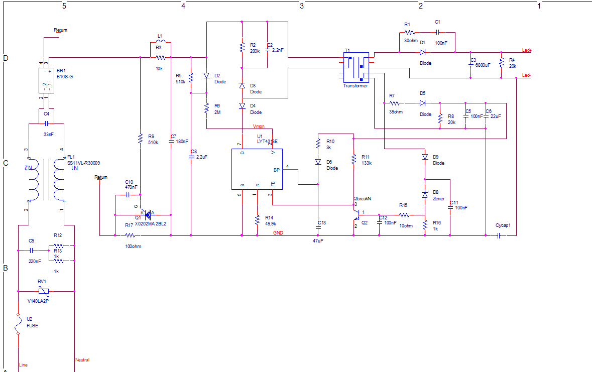
I am working on a 14W, 8-14V, 1A dimmable constant current driver. I have been using DER350 as a reference for the most part. I am trying to figure out what voltage zener diode to use for the overvoltage protection circuit. In DER 350 they use a 33v zener diode, while the output voltage is 36v. The output voltage is sensed via the bias winding which is set to 25v nominally. If I am understanding this correctly the output voltage for the secondary would then be limited to about 47v to protect the output capacitors? Is that a correct assumption?
Thanks,
Alex
Comments
Hi PI-Logan,
Thanks for your reply.
I am also noticing significant flicker on the output. It is not flicker visible to the human eye. We test for flicker at lower frequency <300Hz (per CA title 24 regulations) using a light sensor. I am measuring high amounts of flicker (70%) in the 120Hz area. Is there a way to remove this flicker (down to <20% is the goal.)?
On another note, the output current is much higher than intended, adjusting the FB resistor should change that but I am not entirely sure as to how that is calculated. Any help on this would be great.
Edit: I tested the output current and bias voltage per the design guide instructions. However because the output current is outside the 10% target range, PIXI generates a warning and suggests a 4Mohm resistor for RV. However that change would increase the output current. What are my options to correct this issue?
Thanks,
Alex
| Attachment | Size |
|---|---|
| Schematic | 38.32 KB |
Hi Alex,
For the flicker issue, in what condition do you see this flicker? Is it during full load non dimming conditions? Or when you use the triac dimming functionality?
For your output current regulation issue, you can try fine tuning it by referring to this application note on LYTSwitch-4 (step 11, page 17):
https://led-driver.power.com/system/files_force/product-docs/an59.pdf
Hi PI Logan,
The flicker issue is during full load under non dimming conditions with an output voltage of nominal 12v led at 1280mA current. The current however is slightly higher than than the intended 1000mA due to the current regulation issue. Based on the output waveform it seems like the output voltage is fluttering at the edge of the minimum Vf for the led (10v).
Hope you are enjoying the holidays.
Thanks,
Alex
Hi Alex,
Sorry for the late reply. Since the flicker issue is at non dimming conditions, we can assume that it has nothing to do with the dimming mechanism. Based on your earlier reply, the flicker is around 120Hz. This is most likely due to the rectified input reflecting onto the output. You can either increase the bulk cap C7 (this may affect PF) and see if the flicker is reduced, or you can tweak R5 and C8 which, according to DER-350, prevents rectified line frequency ripple. Hope this helps.
https://led-driver.power.com/sites/default/files/product-docs/lytswitch-4_family_datasheet.pdf
Hi PI-Logan,
Thanks for getting back to me. I tried both of those options and they seemed to help, but only in small amounts. I increased the capacitance of C6 and that also helped a little. The combination of the two changes and the increase in C6 seemed to have fixed the problem. The measured flicker isn't completely gone but it is under the requirement for our application so that is a plus. Thank you very much for your help in solving this issue.
Alex
Hi,
So I was able to fix the previous problem and get the correct output as designed. However, I redesigned the PCB layout to fit in the application form factor and the same circuitry no longer functions properly. I understand that PCB layout is critical in a SMPS design. Are there any places in the layout that I should be weary of? I would expect some relatively minor differences due to layout but the output I am getting is only 400mA when it is supposed to be 1000mA @12V nominal.
Design values:
Vo = 12V
Vin = 85-132Vac
Io = 1000mA
Actual values:
Vo = 10V
Vin = 118vac
Io = 400mA
Any help on this is greatly appreciated, Thanks.
Alex
| Attachment | Size |
|---|---|
| Capture.PNG | 38.32 KB |
Hi Alex,
There are layout considerations stated in page 11 of the product datasheet. To give you more specific help regarding the layout, is it possible for you to provide the new and old layout files (or pictures in pdf format)?
Datasheet: https://led-driver.power.com/sites/default/files/product-docs/lytswitch-4_family_datasheet.pdf
Hi Pi-Logan,
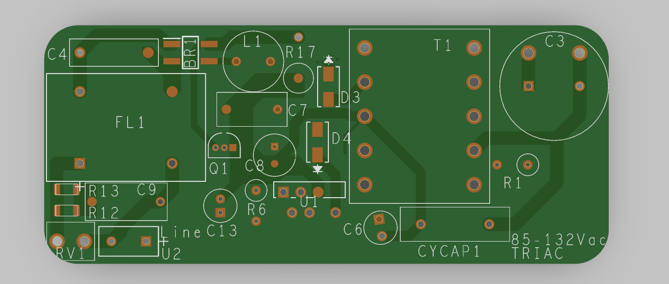
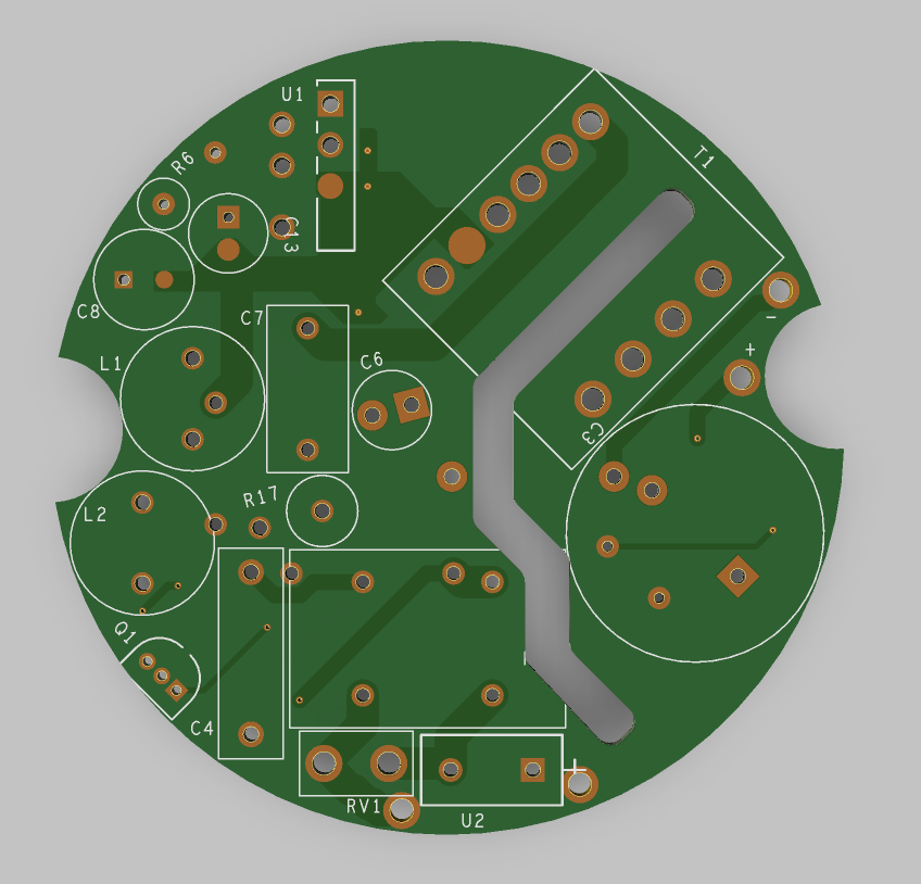
Yes, attached are the layout files in both revisions. The only difference in the circuit were some optional EMI filter components that were not loaded and an optimized transformer.
This was done to test different filter performance. This includes components: L1,R18, and C14.
The transformer however was what I expected to be the problem at first and removed it, replacing the original transformer back in the circuit, still had the same problem. Much lower output current along with what seemed to be poor line regulation.
Thanks,
Alex
| Attachment | Size |
|---|---|
| Circuit_Schematic_for_both_layouts_minus_optional_EMI_filter_components.PNG | 38.32 KB |
| Layout_Version_1_Bottom.PNG | 73.92 KB |
| Layout_Version_1.PNG | 93.35 KB |
| Layout_Version_2_Bottom.PNG | 131.33 KB |
| Layout_Version_2_Top.PNG | 123.16 KB |
Hi Alex,
Sorry for the late reply. It was a bit difficult spotting errors on the layout using images. Although, i spotted one, i think. Please recheck the connection of your auxiliary circuit. It seems that in Version 2, D5 cathode is connected to the return GND. Also, if possible may you send waveform captures of the output. It may help to see how the output behaves. Will continue checking the layout and update you if I see anything suspicious.
| Attachment | Size |
|---|---|
| Layout_Version_2_Bottom.png | 154.45 KB |
Hi Alex,
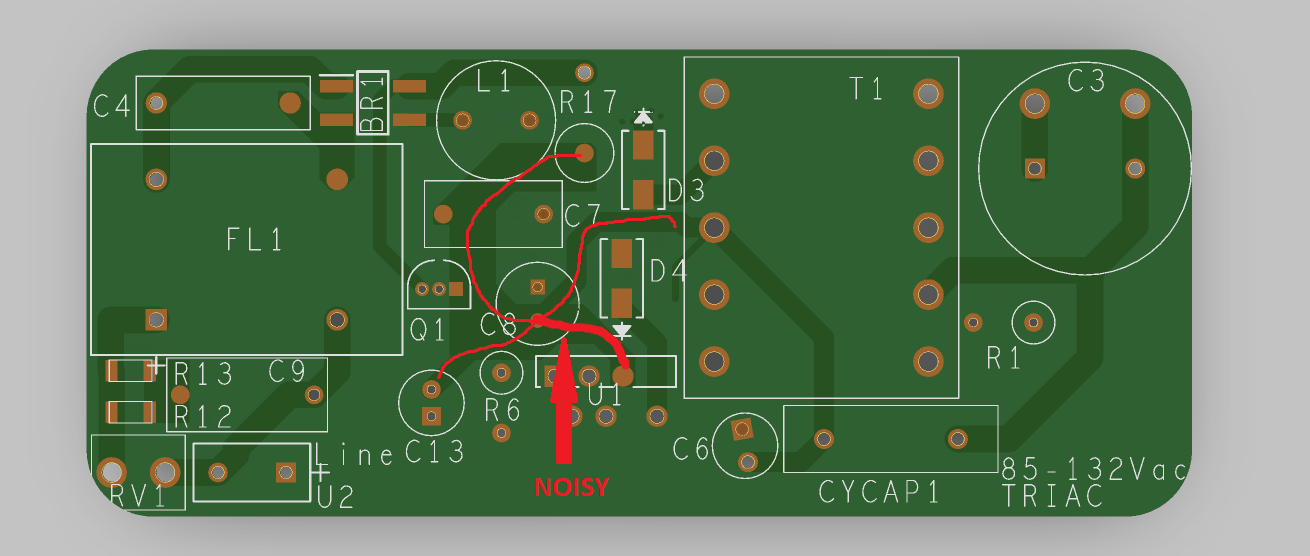
Upon further check, I saw that I was mistaken with my first comment. D5 was routed properly so that is not the problem. Even so, there are a few things I spotted.
- Power GND loop should be as short as possible. C8 is routed further away from SOURCE pin in Ver. 2. Also, important control GND points are put in between and might be affected by noise.
- FB pin connection to Q2 (which facilitates output regulation) is put close to switching node of D3 and D4. It might be affected by noise.
Hi PI-Logan,
Thanks for getting back to me. I am working on getting you those waveforms.
So it is possible that the switching noise created by D4 D3 node is coupling into the FB trace? If that is the case then I probably shouldnt have that loop routed between all 6 pins of the Lytswitch-4. That could be causing a lot of noise issues.
Edit:
After cutting the switching trace running between the pins on the Lytswitch-4, the output improved drastically.
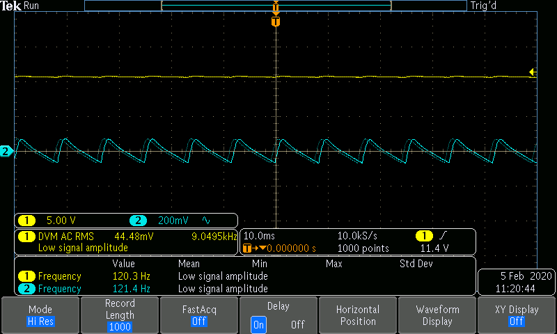
I am seeing 785mA which is still lower than the intended 1000mA but there is much less flicker/flutter issues.
The flicker/flutter issues only seems to happen at full output (785mA).
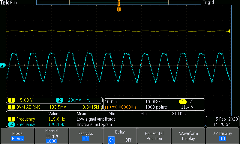
Attached are the output waveforms.
Channel 1 (yellow) shows DC+RMS
Channel 2 (blue) shows output ripple
It seems I am still getting 120Hz albeit not very much, but I would still like to reduce this further.
I am still unsure why the current regulation is lower than the intended output.
Hopefully this is enough info for you. Let me know if you need to see a different waveform from somewhere else in the circuit.
Thanks,
Alex
| Attachment | Size |
|---|---|
| Full_Dimming_Output_Waveform.png | 14.84 KB |
| Max_Load_Output_Waveform.png | 17.42 KB |
Hi Alex,
Thank you for those waveforms. I suspect that there is still noise being coupled on to the feedback/control circuit of the system. One of my suspicions is that the the Version 2 grounding is the problem. If you would look at Version 1, the GND is star grounded to C8. For Version 2, the other ground connections (e.g. sensitive control loops) are placed in between the SOURCE pin and C8. Noise may be coupled on to these control loops and may be causing malfunction.
| Attachment | Size |
|---|---|
| Layout_Version_2_Top.png | 141.63 KB |
| Layout_Version_1.png | 96.16 KB |
Hi Pi-Logan,
It does seem that noise is still being coupled into the FB. I probed the FB line closest to the C8 return and it has a significant amount of noise on it. I will redo the layout with that in mind.
Thank you very much for your help.
Alex
Hi Alex,
Yes, that would be the correct assumption. You need to size the zener diode depending on the output capacitor voltage rating, and the bias winding to secondary winding turns ratio.