
TFS7701H not startup
Why the voltage of Pin BP is still 4.8V, when input voltage exceed 100V, even 300V? it means the Flyback is not working.
Resistors connected to L and R is 3.92M. voltage on L and R is 2.2V and 1.8V. Current limitation resistor is 232k.
could any expert give me some tips? Thank you!
댓글
When I adjust tfs7701, pfc is not assembled, Input voltage is increased from 0 to 220vac. 7701 is not working as expected. The Standby power doesn't work.
| 첨부 파일 | 파일 크기 |
|---|---|
| Pfc | 70.68 KB |
| Two switch | 113.62 KB |
no comments? experts?
Hi,
I found few issues with the schematic.
Replace R39 (7.5 KOhm) with the attached circuit.
You should regulate the Vcc to the PFC at ~12V . If you directly connect VAU15 to the Vcc of the PFC IC there is a chance that it can damage the PFC IC and pull down the standby section.
Take a new board and try this circuit and cut the trace from VAU15 to VCC of PFC IC.
Initially do not populate the 10 Ohms resistor which was shown in the attached circuit. See if the standby section powers up. If it powers up then populate the 10 ohms resistor which was shown in the attached circuit.
Regards,
PI-NANO
| 첨부 파일 | 파일 크기 |
|---|---|
| Linear Regulator | 19.36 KB |
Thanks a lot, PI-NANO. I'll try as your suggestion later.
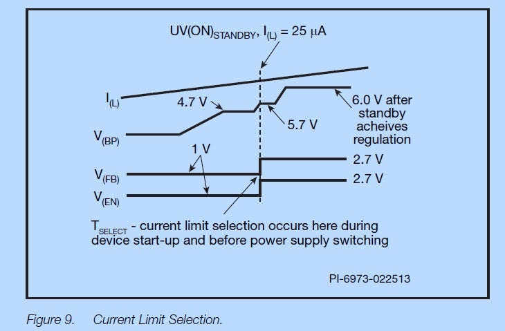
BTW, I have tried to remove R39(7.5K) to see if BP could rise to 5.7V (VAU15 to PFC has been cut off) . The result is BP stays on 4.7V forever, even input is more than 300Vdc. I'm not sure if the IC is broken, but after try with new IC, the behaviour is the same. The other phenomena is the EN is 3.5V, even BP is still 4.7V. it doesn't meet the curve on page 10 in hipertfs-2_family_datasheet. And there's 2 mistakes in this curve, 2.7V should be 3.5V which described on top of page 12. And the selection time is at beginning of 4.7V achieved.
----
The current limit selection for both FEEDBACK pin and ENABLE
pin takes place when the BYPASS pin first reaches 4.7 V. Once
the short detection period is complete, the BYPASS pin is
ramped on up to 5.7 V, and the FEEDBACK pin is allowed to
float to it’s nominal voltage of 3.5 V.
-----how to understand this paragraph? Does it mean if BP stays at 4.7V, EN and FEEDBACK could not go to3.5V?
| 첨부 파일 | 파일 크기 |
|---|---|
| startup sequence in datasheet | 67.72 KB |
Hi,
You have to replace R39 with the attached linear regulator circuit. You can not simply remove R39. You have to supply bias supply to the BP pin.
If you have new board try it on the new board.
If BP pin stays at 4.7V, then EN and FEEDBACK pin are clamped at 1V and standby can not start.
BP has to reach 5.7V in order to release EN and FEEDBACK pins.
Regarding 2.7V vs 3.5V let me go through the data sheet one more time and see if there is some mistake.
Could you please send your magnetics design documents as well.
If you need help with debugging your power supply, contact one of our field office in your geographical location.
Regards
PI-NANO
At first startup of a new design I have shortcircuit the feedback Optocoupler U1B ( Based on DER 368 or fig.30 in the manual )in order study the standby controller without firing the main controller.
Thats is: FB is at ground level from start.
BP ramps up and stays at 4.7V with no rise to 5,7V.
Why ?
If this is a problem for rising BP kindly suggest an alternative approach just starting the standby controller and not the main one at this initial lab test.
Also: Kindly explain the current path for charging BP/C12 at power-up.
Current flow via R1>T2>DSB or ?
Regards,
Tomasf
Hi,
You should not short circuit the feedback pin.
If you don't want to turn on the main, just apply 120VDC at the DC bus capacitor.
It will not turn on the main controller at that voltage. Main controller starts at about 340VDC.
If you need help with debugging your power supply, contact one of our field office in your geographical location.
Regards,
PI-NANO
Hi,
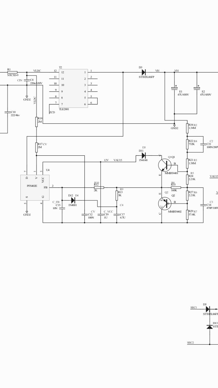
Could you please share your schematic?
Regards,
PI-NANO