
DPA425GN component burnout
This is very agent issue.
We need to place an order for PCBs for mass production in the first week of January.
Please review as soon as possible.
The DPA425GN part is being used as an LED driver in mass production.
Sometimes, drain and source burnout occurs, and this has occurred on several units to date.
I'd like to request a review of the circuit diagram to see if there are any issues. (A comprehensive circuit review is required.)
For reference, this circuit diagram was designed for the TOP414GN in 2018 and was discontinued during mass production, so it has been changed to the DPA425GN.
1. The datasheet states the input voltage is 16-75 VDC and the maximum drain voltage is -0.3 V to 220 V.
- The current circuit also shows a peak (overshoot) voltage of approximately 230 V at a 50 V input, and a normal voltage of approximately 80 V to 95 V.( attached scope picture)
- Could this cause problems due to the continued stress on the DPA425?
2. In the circuit diagram, pins 2 ("L") and 3 ("S") are shorted.
In this case, will overvoltage and overcurrent checks for the input not be performed? Could this cause problems?
3. In the circuit diagram, pins 4 ("X") and 3 ("S") are shorted.
Will this cause problems since overvoltage and overcurrent checks for the secondary output not be performed?
4. I believe the lack of a primary-side drain and secondary-side output snubber circuit is contributing to the high overshoot rate.
I would like to request a circuit review and improvement plan for this area.
5. Are the D6 and D5 component circuits necessary? Please consider replacing the Drain and Source with SMBJ150A (STAND-OFF VOLTAGE 150V).
6. The transformer data sheet is attached. Please also review the matching of the DPA425 and the transformer.
7. I need to place the final PCB order in the first week of January. If I need to use the DPA425GN, I would like to request a solution.
8. Additionally, I would like to request the most optimal component and circuit configuration instead of the DPA425. (I tried using PI Expert Online, but could not find an accurate solution.)
9. The FET1 (FCP130N60) block initially consumes 450mA (PC1-A) and then 275mA (PC1-B) at normal operating conditions. This current is dissipated through an 18-ohm resistor.
I would also like to request a review of this.
回應
Dear Tommy
Thank you for your quick reply.
I have additional questions.
1. Can I improve the Lpri Gauss value of the transformer by using the same transformer and connecting a 15K resistor (controlling the output current of 600mA) to the X pin to lower it below 3000?
If I need to replace the transformer, please recommend a suitable commercial transformer manufacturer or part number.
2. Additionally, what about limiting the input current by connecting a 619K resistor between the L pin (No. 2) and the input voltage? (This is how it is applied in your app data.)
3. I have attached the circuit layout drawing. Please review it for any issues.
Thank you
Jongho Park
| Attachment | 大小 |
|---|---|
| (CSCB-ART-A-17) 색등식 LED 신호기 제어부 PCB V1.7.pcb (1.21 MB) | 1.21 MB |
Hello Jongho Park,
Good afternoon and thanks for your mail.
To answer your additional questions, please refer below.
1. Can I improve the Lpri Gauss value of the transformer by using the same transformer and connecting a 15K resistor (controlling the output current of 600mA) to the X pin to lower it below 3000? If I need to replace the transformer, please recommend a suitable commercial transformer manufacturer or part number.
- Implementing an X pin resistor will certainly lower the peak flux density value of the transformer. However, even if we use a higher resistance on the X pin resistor, it's still not enough to reduce it down below the recommended 3000 Gauss value due to the number of turns of the secondary winding (14 turns).
- For the new transformer, what I can suggest is to reach out directly to your transformer manufacturers to see if they can make the custom transformer that is included in the PDF file that I shared previously (15V_0.5A_DPASwitch_Initial_Flyback.pdf).
- If you don't have a transformer manufacturer, you can browse through one of the transformer vendors listed in this link (component suppliers) that is nearest to your location.
2. Additionally, what about limiting the input current by connecting a 619K resistor between the L pin (No. 2) and the input voltage? (This is how it is applied in your app data.)
- Adjustment of the input current/current limit is done through implementing an X pin resistor. Placing an RLS resistor (619 K ohms) between the L pin and +HV rail will only set the UV and OV threshold levels around 33.3 V and 86.0 V, respectively.
3. I have attached the circuit layout drawing. Please review it for any issues.
- Unfortunately, I cannot view or download the PCB attachment you have shared. May I kindly request if you could try putting it in a zip file, and I'll check if I can download it on my end?
Thank you and I wish you a great day ahead!
Best regards,
Tommy
Dear Tommy
Thank you for review about that.
1. It seems like it will take a lot of time to proceed with the new transformer you guided.
Ultimately, we plan to consider building a new transformer.
However, due to the tight schedule, we are currently looking for ways to improve the existing transformer.
- Method 1) Using this transformer and the DPA425 (through protection elements on the surrounding X, L, and C pins)
. X pin: Connect a 15K resistor
. L pin: Connect a 690K resistor
. Add a protection element to the Drain pin
- Method 2) Using this transformer and the new DC/DC converter (Please recommend pin-to-pin components first, and then request secondary component recommendations and a schematic.)
-> I would appreciate your guidance on these two methods.
2. I am sending you our PCB layout in pdf format.
Please review.
Thank you
Jongho Park
| Attachment | 大小 |
|---|---|
| LED PCB_layout_20260107.pdf (240.11 KB) | 240.11 KB |
Hello Jongho Park,
Good day and I hope you're doing well.
I understand the timeline of the design. However, unfortunately for method 1, the transformer is still not suitable for the design even if we implement an X pin and L pin resistors on the design because the peak flux density value is still high (which might lead to core saturation during operation). For method 2, we don't have any device that is pin-to-pin compatible with the G package of the DPA Switch.
That said, here are the options that I recommend:
- Replace the current transformer with a new one.
- If you really wish to use your current transformer, switching to TOPSwitch-JX (TOP271EG) is suggested. However, this will require some modifications to the layout since the package of the IC is different from the DPA Switch. Please refer to the attached file for the initial design using the TOP271EG device and an EI19 core/bobbin. Another thing I strongly suggest is to consult with your safety engineer if your current transformer meets the isolation requirement between primary and secondary because I noticed in the transformer datasheet you have shared that all windings use the same type of wire (2UEW).
Thank you and I wish you a great day ahead!
Best regards,
Tommy
| Attachment | 大小 |
|---|---|
| TOPSwitch-JX_PIDesign_15V_0.5A.pdf (2.16 MB) | 2.16 MB |
Dear Tommy
Thank you for your prompt response.
We requested the transformer manufacturer we use and are sending you the transformer specs with some modifications.
We would like to request another simulation for DPA425 integration.
Please review for any issues with Gauss and magnetic flux density.
Changes
1. Core type: EL1916 -> EE1916
2. Primary turns: 69 & Inductance: 285uH
3. Secondary turns: 36
4. Feedback turns: 30
attached transformer datasheet
Thank you
Jongho Park
| Attachment | 大小 |
|---|---|
| EE1916_modified_transformer_260107.pdf (394.59 KB) | 394.59 KB |
Hello Jongho Park,
Good day and thanks for sharing the new transformer file.
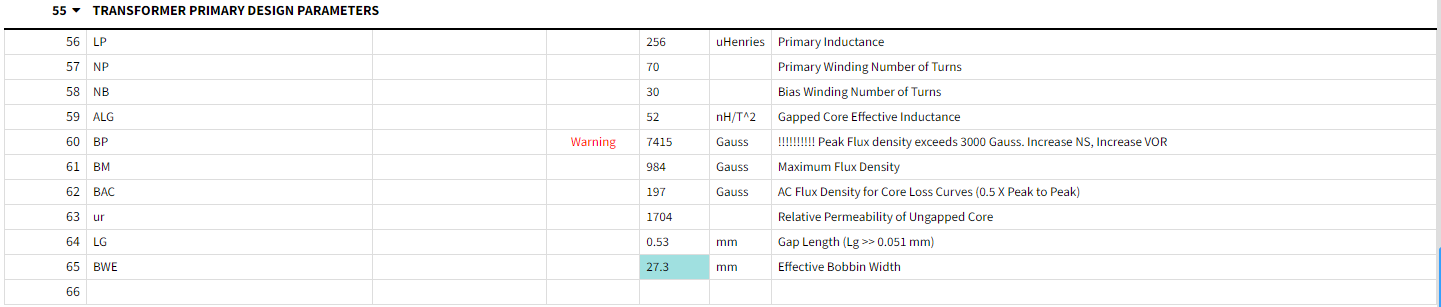
Upon verification of the new transformer on our PI Expert Online (XLS spreadsheet), the spreadsheet still shows a warning on the peak flux density with a value of 7415 Gauss. Kindly refer to the attached image for your reference.
A larger transformer like EFD25 or equivalent is recommended to be able to resolve the peak flux density warning. Please see the attached file for your reference.
Thank you and best regards,
Tommy
| Attachment | 大小 |
|---|---|
| EE19 Transformer.png (45.92 KB) | 45.92 KB |
| 15V_0.5A_DPASwitch_Initial_Flyback (2).pdf (1.25 MB) | 1.25 MB |
Dear Tommy
We've been conducting additional testing for several days.
We're testing each LED color, and we've noticed something unusual.
The RED LED (operating 180 LEDs) requires a low output voltage (9.5V), while the GREEN LED (operating 180 LEDs) requires a high output voltage (14.5V) to meet the specifications. (attached DPA425GN_Test for LED colors_260113.pdf)
The output voltage is controlled by a variable resistor via a low feedback resistor. (attached DPA425GN_DCDC Block_For PI_260113.pdf)
- 4.2K: VCC Out 9.5V (RED LED)
- 2.8K: VCC Out 14.5V (GREEN LED)
1. In this case, the RED LED has a consistent on time, but when driving the GREEN LED, the DPA425 turn-on time (400ns~630ns) keeps fluctuating. Please review this issue and suggest further improvements.
2. Please also inform the minimum duty cycle for working in our circult.
3. Additionally, we would like to test a transformer made with the same EFD25 type, materials, and specifications you suggested. In this case, can the R, L, and C values around the transformer be the same as those of the existing EI1916 transformer, or if the time constant needs to be changed, please let us know.
Thank you
Jongho Park
| Attachment | 大小 |
|---|---|
| test result for LED colors (395.32 KB) | 395.32 KB |
| schematics for DPA425 (230.67 KB) | 230.67 KB |
Hello Jongho Park,
Good day and I hope you're doing well.
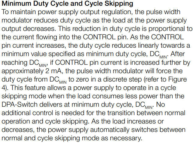
The phenomenon you have observed when operating the power supply at both 9.5 V and 14.5 V is normal. The way that the DPA Switch device maintains the output voltage in regulation is by varying its duty cycle depending on the input voltage and output power. You can refer to the attached image for detailed information regarding the minimum duty cycle and cycle skipping (this can also be found on page 6 of the DPA Switch datasheet).
For point number 2, the minimum duty cycle (DCmin) that the device can operate is 4% according to the DPA Switch datasheet.
Regarding point number 3, yes, you can test the new EFD25 transformer while maintaining the same values for other components.
Thank you and best regards,
Tommy
| Attachment | 大小 |
|---|---|
| DPA Switch Minimum Duty Cycle and Cycle Skipping.png (163.92 KB) | 163.92 KB |
Dear Tommy
Thank you for check them.
I attached EFD25 transformer datasheet for DPA425GN DCDC convertor.
Check it please.
Thank you
Jongho Park
| Attachment | 大小 |
|---|---|
| EFD2525_Transformer_20260114.pdf (175.08 KB) | 175.08 KB |
Hello Jongho Park,
You're very welcome.
The transformer design specifications of the attached file look great. Let me know the results once testing is done on your side with this transformer.
Thank you and I wish you a great day ahead!
Best regards,
Tommy
Yes, I will test about that in this week and going to share it to you.
Thank you
Jongho Park
Dear Tommy
I'm sending you the waveforms and schematic changes tested with the finalized transformer. Please review them carefully.
I'd like to request your feedback today.
Also, the drain waveform appears to be a sine wave after turn-off. Is this a problem?
Thank you.
jongho park
| Attachment | 大小 |
|---|---|
| LED DCDC Convertor Burnt검토_260116_pi.pdf (947.94 KB) | 947.94 KB |
Hello Jongho Park,
Thanks for sharing the latest schematic and results of the actual test with the new transformer. It's great to see that the drain-source voltage of the DPA Switch device is not exceeding the 220 V absolute maximum voltage anymore.
Since you already added the SMBJ150A and 330 pF (cases 5 and 6) between the drain and source pins, D5 and D6 can be removed from the circuit. The addition of 10 ohms and 330 pF (case 10) on the circuit was also good. You may now select an output rectifier with a lower voltage rating (150 V to 200 V) for cost reduction (if you choose not to change the output rectifier, it's also fine). The implementation of the X-pin resistor (case 11) was also fine. For case 12, the new overvoltage threshold is around ~95 VDC with UV functionality disabled. In summary, the schematic and results look great.
Then, to answer your question, no, it's not a problem and a normal behavior of the flyback converter. When the DPA Switch device turns off, the energy stored in the transformer's leakage inductance has nowhere to go immediately. This energy causes a voltage spike and then resonates with the Coss of the DPA Switch IC and other stray capacitances on the circuit, creating a characteristic damped oscillation (ringing) on the drain-to-source voltage waveform. For additional reference, you may check page 16 of the DER-30.
Let me know if you need further assistance or have any more questions or clarifications.
Thank you and I wish you a great day and a relaxing weekend ahead!
Best regards,
Tommy
Dear Tommy
I'm contacting you with an additional question regarding a problem with temperature testing based on the last shared circuit diagram.
When testing with 50V DC as the transformer input and the temperature set to -40°C, the secondary output 14V does not output properly and the circuit keeps resetting.
It operates fine at room temperature (consumes approximately 14V/500mA).
The outdoor operating conditions for this product are -40 to +70.
I'd like to know if I need to adjust the time constant on the X pin or the primary side.
Thank you.
Hello Jongho Park,
Good day and I hope you're doing well.
One thing I noticed in the schematic diagram is that the current optocoupler of the design (TLP521-4) is only rated for -30 °C. There is a high chance that this might be the reason why the design is continuously restarting during -40 °C ambient temperature. I’d suggest replacing it first with a part that has similar CTR specifications but is rated for -40 °C or below.
In that regard, I also recommend double checking the operating temperatures of each component and ensure that it is rated appropriately.
Thank you and I wish you a great day ahead!
Best regards,
Tommy
Dear Tommy
I have an inquiry regarding the circuit.
This is the circuit diagram I previously inquired about. While there are no operational issues, there is a problem regarding current consumption.
This product has specific current consumption specifications, but we are currently failing to meet them.
The constant operating current should fall within the range of 110mA to 150mA based on an input voltage of 50V, but currently, the current needs to be reduced to around 200mA.
When checking the current by block, the results are as follows.
| DPA425 Current measure(03/20) | |||||
| title | 5V(mA) | 15V(mA) | 50V(mA) | 50V(mW) | |
| 1 | Input Voltage 50V (Total) (mA) | 200.7 | 10,035 | ||
| 2 | DCDC convertor (DPA425 Block) (mA) | 6,994 | |||
| 3 | 5V Block(mA) | 60.1 | 301 | ||
| 4 | 15V LED Module Block (mA) | 182.7 | 2,741 | ||
It is estimated that the DPA425 block is consuming a significant amount of current.
I request a review of the efficiency based on the current circuit diagram and areas for improvement.
Since we need to reduce the current by at least 60mA/50V, I am requesting this review urgently.
Thank you.
Attachment: DPA425_Schematic_To Powerint_260320.pdf
| Attachment | 大小 |
|---|---|
| DPA425_Schematic_To Powerint_260320.pdf (107.18 KB) | 107.18 KB |
I have an additional question regarding the previous one.
The measurement table above was taken with the Load Register block disabled.
It is estimated that the DPA425 block is currently consuming a significant amount of current.
Additionally, the circuit diagram shows the current being routed to ground through resistors R14 and R15 (total resistance 18 ohms). Changing this resistor value to 50 ohms improves the current by reducing it from the existing 200mA/50V to 183mA/50V, a decrease of approximately 17mA.
However, in this case, as the resistance value increases, the voltage on the DPA425 pins 5, 7, and 8 rises to 2.6V.
I request that you verify the circuit and the direction for improvement regarding this issue.
Thank you.
Jongho Park
Dear Tommy
I am submitting this third inquiry because I was unable to edit the email sent above.
When modifying the DPA425 circuit last time, I added a snubber circuit and requested confirmation regarding whether these circuits are causing a decrease in efficiency.
There appears to be some loss in the R36 (10 ohms) and C28 (330pF) circuits on the secondary side.
I request a review to see if there are any improvement suggestions for the added circuits.
Thank you
Jongho Park
Hello Jongho Park,
Good day and I hope you're doing well. Apologies for the delayed response, as we were on holiday last Friday (March 20).
Regarding the current consumption, are you referring to the input current during no-load? or you are looking for some ways to improve efficiency at 50 V input during full load condition? I would really appreciate it if you could clarify.
May I also ask the purpose of resistors R14 and R15 and capacitor C7 on the circuit? Are the mentioned capacitor and resistors necessary? The RTN ground of the DPA Switch along with D12, C29, R37, C8, C6, and C9 should be connected to the GND of the input capacitor C11 and C19.
Thank you and looking forward to your response.
Best regards,
Tommy
Hello Jongho Park,
Good day and I hope you're doing well. Happy new year!
The TOP414GN and DPA425GN is a totally different product family therefore, they cannot be a direct replacement for each other. Since they also have their own distinct parameters and ratings (for example current limit, switching frequency, duty cycle, etc.), some components may not be suitable when the DPA425GN was used, especially the transformer.
To answer your questions, please refer below.
1. The datasheet states the input voltage is 16-75 VDC and the maximum drain voltage is -0.3 V to 220 V.
- The current circuit also shows a peak (overshoot) voltage of approximately 230 V at a 50 V input, and a normal voltage of approximately 80 V to 95 V.( attached scope picture)
- Could this cause problems due to the continued stress on the DPA425?
2. In the circuit diagram, pins 2 ("L") and 3 ("S") are shorted.
In this case, will overvoltage and overcurrent checks for the input not be performed? Could this cause problems?
3. In the circuit diagram, pins 4 ("X") and 3 ("S") are shorted.
Will this cause problems since overvoltage and overcurrent checks for the secondary output not be performed?
4. I believe the lack of a primary-side drain and secondary-side output snubber circuit is contributing to the high overshoot rate.
I would like to request a circuit review and improvement plan for this area.
5. Are the D6 and D5 component circuits necessary? Please consider replacing the Drain and Source with SMBJ150A (STAND-OFF VOLTAGE 150V).
6. The transformer data sheet is attached. Please also review the matching of the DPA425 and the transformer.
7. I need to place the final PCB order in the first week of January. If I need to use the DPA425GN, I would like to request a solution.
8. Additionally, I would like to request the most optimal component and circuit configuration instead of the DPA425. (I tried using PI Expert Online, but could not find an accurate solution.)
Then, another thing I noticed on the schematic diagram is that the circuit doesn't have a lower feedback resistor connected between R11 and secondary GND. Without a lower feedback resistor, the power supply will not regulate to its desired output voltage, and the device will trigger its auto-restart function. With a reference voltage of 1.24 V for the TL431ALPG and 30 kΩ upper feedback resistor, adding a lower feedback resistor of around 2.7 kΩ is strongly recommended.
Thank you and looking forward to your response.
Best regards,
Tommy