

weired voltage wave on Pin S of LNK306GN
HI PI
I use LNK306GN for a buck topology with 6.8V DC @260mA(peak current) output, 86V DC input . When LNK306GN is at light load, I find a weired voltage wave on Pin S of LNK306GN. There is a continous oscillate around 6.8V as the attachment shows. In my opinion, maybe there is no current flow through Inductor. So voltage on Pin S should equal to output voltage. But it is not. Is this proper? Thank you. P.S. the yellow wave is output voltage, the green wave is voltage on Pin S.
Comments
Is anyone can reply me? It is really emergiency. Thank you.
Hi Arthur,
Can you also capture inductor current vs source voltage and zoom further.
The oscillation may be due to the BPP/ control feedback and freewheel diode.
Regards
Hi Data,
You mean this wave is actually weired? I will give you the related voltage zoomed later.
I am not sure actually but if it is working fine then you should not be worried. Can you also capture wavefom during full load and half load.
Thanks.
Hi Data,
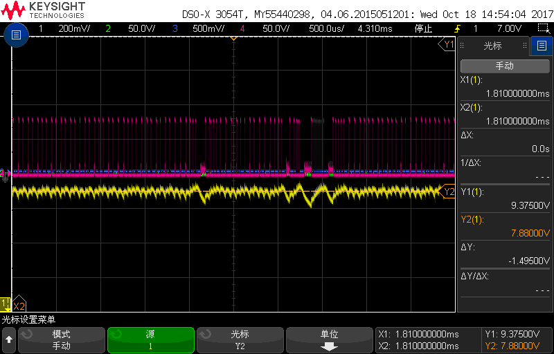
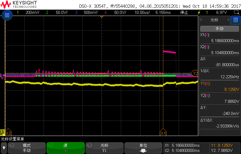
We don't have current probe, So we can't probe inductor current. We just capture Pin S voltage and output voltage which we set as 7.9 VDC. And the full load is a 40 ohm risistor with the load current is about 200 mA, the half load is a 80 ohm risistor with the load current is about 100 mA. The attatchment is the related voltage. The red wave is voltage of Pin S. The yellow wave is output voltage. With full load, we think LNK306GN works at CCM mode. But we find sometimes it still works at DCM mode. And the output voltage ripple changes a lot about 200mV. But usually it works at CCM mode. With half load, there is a continous oscillate around 7.8 VDC as i mentioned before, We try to serial a risistor 1ohm with inductor. We want to obtain current by probing voltage between the terminal of this risistor. But we find there is a loud noise we can hear from inductor. So we don't know it makes sense. If you think it can work. We will capture inductor current by probe risistor voltage. By the way there is always a light noise we can hear from inductor. We don't know is it proper.
| Attachment | Size |
|---|---|
| 200mA.png (43.87 KB) | 43.87 KB |
Here is the Pin S voltage and output voltage at full load and half load.
| Attachment | Size |
|---|---|
| When LNK306GN works at CCM mode, but sometimes there is also oscillator at Pin S (37.89 KB) | 37.89 KB |
| the proper voltage wave when LNK306GN works at CCM mode. (37.69 KB) | 37.69 KB |
| the proper voltage wave when LNK306GN works at CCM mode. (38.27 KB) | 38.27 KB |
| the proper voltage wave when LNK306GN works at CCM mode. (39.08 KB) | 39.08 KB |
| Half load (46.2 KB) | 46.2 KB |
| Overview (43.92 KB) | 43.92 KB |
| details about oscillator (37.55 KB) | 37.55 KB |
| Overview about oscillator (39.44 KB) | 39.44 KB |
| details about oscillator (40.49 KB) | 40.49 KB |
| details about oscillator (34.44 KB) | 34.44 KB |
Hi Arthur,
The way I see it, there is no problem with the oscillation. It occurs when no energy left on the inductor and the oscillation is caused by output capacitor and the inductor. The output ripple looks normal. For output cap, try to use very low ESR to lower the ripple voltage.
Regards
You mean when it oscillates, is it the right current flow?
| Attachment | Size |
|---|---|
| Picture1.png (31.88 KB) | 31.88 KB |
Hi Arthur,
Yes due to high frequency parasitics.
Regards.
Hi Data,
Thank you for your reply. I have another question.
Ⅰ, I want to use LNK306GN with 18 VDC to 115V DC input and 7.9 VDC output. The maximum output current is 100mA. I do not want your promise or guarantee here. I know the minimum voltage of this IC is 70V DC.
Ⅱ, We used to use your TOP221G as converter in our product for many years. But unfortunately, TOP221G will be in stop production later. So we have to redesign to use for LNK306GN to change this converter. I am not sure whether you have another more suitable IC for our apply.
ⅡI, With low voltage input like 18V DC input, we find the voltage wave of Pin S is not proper. When the mosfet turns on, the voltage of Pin S has a decreasing tendency. I don't know whether at this time the mosfet turns on fully. And the voltage between Pin BP and Pin S I think is sufficient. So I don't know the reason. And the mosefet also turns off for a long time. It cause a large voltage ripple at output. Can you explain it. Thank you. The attatchment is the related voltage wave. The red wave is voltage wave of Pin S. The blue wave is the voltage wave between Pin BP and Pin S. The yellow wave is the output voltage.
| Attachment | Size |
|---|---|
| scope_10.png (55.29 KB) | 55.29 KB |
Hi Arthur,
The ripple is natural due to the ESR of the output capacitor since you are switching and current is flowing into output capacitor. The waveforms on Pin S is really strange. It is possible that during Mosfet turn-on you are measuring the input voltage and the voltage level is depleted due to energy transfer to output.
Regards
Hi Data,
I can't understand you. If the Mosfet turns on, I think the waveform on Pin S should be is all the same to input voltage. But it is different from the input voltage as I showed you before. May be You can have a try if you have a LNK306GN board with 20 VDC input and 8 VDC output@100mA.
Hi Arthur,
You are correct to say that it is the same to input voltage. And what I am saying is that the input voltage is depleted from time to time based on line frequency or cap value.
Hi Data,
But I am sure the input voltage is all the same.
Hi Arthur,
Try increasing the input voltage until you get good PinS waveform to see if at what level and probably you could only get low as that.






Here is my schematic.