

Test Procedure for DPA424 Based Power Supply
Dear All,
I have designed a power supply based on DPA424 with input 38 to 58V and output of 12V,1.5A and 18V,0.3A. I want to test the hardware prototype developed. What is the general test procedure and at what load I should keep for initial test (say 10% etc). What key waveforms should be observed .
Thanks & Regards,
コメント
Hi Tommy,
Thanks for your reply.
I tested the system, at light loads (i kept 100 ohms for 18 V supply (Design Rating of 0.3A) , and 30 ohms for 12 V output (Design Rating of 1.5A). Initially, it was working with some blinking. The outptut was 7 volts. I tried to adjust the feedback voltage using potentiometer in the circuit. However, now the system is not working at all under any setting of potentiometer. The intial waveform and waveform of control pin when there is no output is attached.
| Attachment | サイズ |
|---|---|
| Waveforms when the secondary showed some output (49.5 KB) | 49.5 KB |
| Control Pin Voltage and Input Voltage (29.46 KB) | 29.46 KB |
Hello sachindevassy,
Thanks for providing the waveforms. If you have an output LED and it is blinking, it means that the device is triggering the auto-restart function and is seeing a fault. By the looks of it, the 7 V output you're getting for the green waveform is just the noise picked up by your probes. If you will observe the waveform, the spikes on both output voltages are in-sync with the drain-source voltage waveforms.
It would be great if you could share your actual schematic diagram, PI Expert file (if there is one), and actual transformer datasheet from the manufacturer so I can review and check if there is anything unusual with the parameters and component values.
Some questions:
- What topology are you currently using? Is it flyback or forward?
- Did you refer to any of our design examples on our website (power.com)? If yes, can you share the link to the design example you referred to?
Looking forward to your response. Thank you.
Regards,
Tommy
Dear Tommy,
Thankyou for the reply.
I am using Flyback Topology and has two desired outputs V1= 12V @1.5A , V2= 18V @ 0.3A.
The PI Designer reference schematic (Fig1) is attached and its transformer data (Fig2) is attached.
The Developed Schematic (Fig 3) is attached and its Layout (Fig 4) and transformer construction data (Fig 5) is attached.
There is a mistake in 18 V winding (which I realized today).
A new board was tested today with an even lighter load
At V2 load connected is 100Ohms
At V1 load connected is 50 Ohms
Under this condition, the 12V output is functioning properly and 18V is giving approx 7V (this is also right as there was a mistake in winding). The waveform is attached.
However, when the load for 12V output was changed to 25Ohms, the converter stopped giving output after few cycles.
The control pin voltage is attached.
Yesterday similar issue happened with the first board. We changed the device (DPA), opto, TL431 and pot but it didn't work and also there was no damage to the tracks.
What could be the issue and how to diagonize this.
Also based on my transformer polarities/connection, the 18V winding should have more turns than 12V . Here, I have used 3 turns for 18V transformer output (as per PI transformer data). I overlooked the connection of transformer.
Are there any spice models for the DPA424 to simulate the behavior of the supply.
Thanks & Regards
| Attachment | サイズ |
|---|---|
| Fig 2 (52.68 KB) | 52.68 KB |
| Fig1 (65.21 KB) | 65.21 KB |
| Fig 4 (42.65 KB) | 42.65 KB |
| Fig 3 (43.75 KB) | 43.75 KB |
| Fig 5 (103.91 KB) | 103.91 KB |
| 12V_with_50Ohm_load.png (74.38 KB) | 74.38 KB |
| Control_Pin_Voltage_undernotworking.png (136.38 KB) | 136.38 KB |
Hello sachindevassy,
Thank you for the design files. Unfortunately, there is no spice model for the DPA Switch.
Have you also checked the transformer's actual primary inductance? It should be around 54 uH, as shown in the "Electrical Test Specifications" in the PI Expert file (Fig. 2).
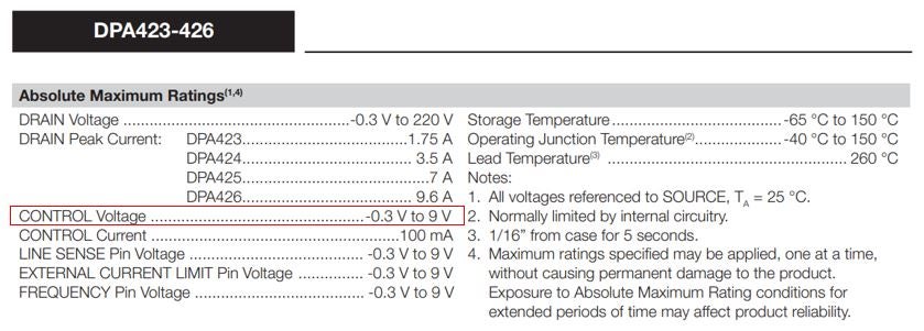
As you have also noticed, the control pin voltage is rising up to approximately greater than 30 V, which means that it is picking up unwanted noise that significantly elevates its voltage level. The C-pin voltage should always be equal to 5.8 V in normal operation and should not exceed the control pin's absolute maximum rating voltage of 9 V (please see attached image) because it will damage the IC. So, there's a high chance that your IC is now damaged and needs replacement.
Since the control pin is picking up unwanted noise that causes its voltage measurement to rise significantly, there's a very high chance that the issue is caused by the layout. The best thing I can suggest is to do a re-layout and follow the "DPA Switch Layout Considerations" that can be found on pages 18–20 of the DPA Switch datasheet and the "Layout Considerations" that can be found on pages 16–17 of the DPA Switch design guide (AN-31).
Here are the some findings and tips based on your layout:
- Remove resistor R34. This will allow you to directly connect the SOURCE pin of the IC to the input capacitor C1.
- As much as possible, do not route a signal trace underneath the IC.
- Place the control pin capacitor C5 adjacent to the IC. That way, you can connect the control pin capacitor directly to the C pin and the SOURCE pin.
- Prevent routing a trace, especially the signal traces, near the DRAIN pin and the traces connected to it as it is a switching node, which is noisy, to prevent noise coupling.
- Keep the primary power loop and secondary power loop as small and compact as possible.
Let me know if you require further assistance or have any more questions. Thank you.
Regards,
Tommy
| Attachment | サイズ |
|---|---|
| Control Pin Voltage (Absolute Maximum Rating).JPG (56.94 KB) | 56.94 KB |
Hi TOMMY BRADFORD
Sorry for the late reply,
I changed the snubber circuit to 7.5k. The system seems to be running in some sort of auto-restart mode. The output voltage is around 6V (desired is 12V).
I am attaching the switching waveform and long-duration waveform of the system. The waveforms captured are (Ch1: Input Voltage, Ch2: Output Voltage, Ch3: Drain to Source Voltage, Ch4: Control Pin Voltage.
The load connected at 12 V terminal is 16 ohms, the load connected at 18ohm terminal is 50ohm. The revised PI diagram is also attached for your reference. The leakage inductance measured is 1uH and the primary inductance is around 60uH. When the load is reduce, the system output voltage becomes higher (around 10V).
Please suggest what changes need to be made further.
Thank
| Attachment | サイズ |
|---|---|
| 12V_18V_updated_18092024.pdf (65.84 KB) | 65.84 KB |
| ExNoote.png (224.17 KB) | 224.17 KB |



Hello sachindevassy,
Good day and thank you for choosing Power Integrations product as part of your design,
For the test procedure, kindly refer to the following step below:.
The key waveforms that need to be monitored during power-up are the drain-source voltage of the DPA424 and the PIV of the secondary rectifier diode. Make sure that their maximum voltages at the highest input voltage with a full load condition don't exceed their absolute maximum ratings (please see their respective datasheets). The rule of thumb here in our lab is to have a margin of 80% for the maximum voltages of both switches at the highest input voltage with a full load condition.
I hope that the above information helps. Let me know if you have any further questions or clarifications.
Thank you and I wish you a great day.
Regards,
Tommy