
TNY286DG-TL is not providing enough Power
I made Pcb circuit of SMPS using TNY286DG-TL which convert universal input (90-250VAc ) to 5V 1.5 I designed a PCB circuit for an SMPS using TNY286DG-TL, which converts universal input (90-250VAC) to 5V at 1.5 amperes. I took help from the PI expert Software.
Here is the Design PI recommended to me
SMPS_Ref_Design_PI_Expert.png
The Schematic of my circuit is
my_Smps_design_schematic.jpg
Now I am sharing the problem I am facing
The circuit is unable to provide the required power.
At no load, I am getting 5V at the output, so the circuit seems to be working correctly.
Case 1 Results:
At a 0.25A test load, the SMPS circuit is providing 0.11A, and the voltage has dropped to 4.18V from 5V.
Therefore, the theoretical power was calculated as 5 x 0.25 = 1.25 Watts, but the SMPS is delivering 4.18 x 0.11 = 0.4598 Watts.
Case 2 Results:
When testing with a load of 0.69A, the SMPS circuit supplies only 0.12A, and the voltage drops to 3.82V from 5V. The theoretical power in this case was 5V × 0.69A = 3.45 Watts, but the SMPS provides only 4.18V × 0.11A = 0.4598 Watts, which is significantly lower than expected.
I'm puzzled by these results, especially since I have already used a 10µF capacitor at the BP/M pin to extend the current limit to the maximum.
I also used a transformer that I received as a sample from a supplier. I provided them with an Excel sheet detailing the transformer specifications I selected from the PI software, and they manufactured it according to those specifications.
Please review my schematic and circuit, and let me know what the possible issues may be, as I am quite stuck. Thank you!
评论
It is the gerber file of PCB board
| Attachment | 大小 |
|---|---|
| Gerber_PCB1_2_2025-12-01.zip (27.46 KB) | 27.46 KB |
- i used a 120 ohm resistor instead of a 500 ohm resistor.
- i will use a 1 kΩ resistor in parallel with the LED part of the optocoupler as you recommended
-
Is the 120 ohm value still too high for the design, preventing the optocoupler from transferring enough current to pull low the EN/UV?
I provide the manufacturer of the transformer with the datasheet of the transformer construction recommended by the PI expert. He said I made exactly the same as PDF I provided to him.
TinySwitch-4_PIDesign2 (3) (1).pdf
The actual PI Expert file (in PDF format) of this design
TinySwitch-4_PIDesign2 (1)_0.pdf
Please help us . We will order tny286 chip in bulk if our circuit works.
| Attachment | 大小 |
|---|---|
| TinySwitch-4_PIDesign2 (1)_0.pdf (480.55 KB) | 480.55 KB |
| TinySwitch-4_PIDesign2 (3) (1).pdf (1.09 MB) | 1.09 MB |
Hello Ahtisham@Enfana,
Thank you for sharing the documents requested.
For the schematic and transformer file, I tried replicating it on the PI Expert and it looks fine. However, for the PCB layout of the circuit, there are important findings that needs to be addressed. Kindly refer to the attached file for our feedback.
To answer your question #3, the 120 ohms resistor value still depend on the testing to verify the actual performance of the design. If you have any 27 ohms to 47 ohms resistor there, then it would be a better option.
Thank you and let me know the results of the testing when the resistor R6 is reduced.
Best regards,
Tommy
| Attachment | 大小 |
|---|---|
| PCB_Layout_Review_TNY286.pdf (1.54 MB) | 1.54 MB |
Hello TOMMY BRADFORD
I replaced the 120-ohm resistor with two 47-ohm resistors, but the results remain the same. Voltage drops at the Load.
I am currently making the second revision of the PCB board; please review it so I can order the PCB for manufacturing.
Schematic is sch_tny286.pdf
Gerber file is Gerber_PCB_Rev2_2025-12-03 (2).zip
Additionally, I measured the voltages at the BP/M and EN/UV pins using a digital multimeter (DMM) with reference to the source. I found that the BP/M to source voltage is 5.95V, while the EN/UV to source voltage is 0.7V at no load. Under load, the voltages drop to approximately 0.38V and 0.58V for EN/UV pins, respectively. According to the datasheet, the EN/UV pin should be at 1.2V.
| Attachment | 大小 |
|---|---|
| sch_tny286.pdf (70.18 KB) | 70.18 KB |
| Gerber_PCB_Rev2_2025-12-03 (2).zip (29.05 KB) | 29.05 KB |
Hello Ahtisham@Enfana,
Thanks for sharing the updated layout. Please refer to the attached file for the new feedback.
As the resistor adjustment to 47 ohms did not improve the design’s behavior, the voltage drop observed at higher loads is likely associated with the layout. Due to the lack of copper heatsink area, the temperature of the TinySwitch-4 IC might be rising significantly, affecting its overall performance. With that said, I strongly recommend fixing the layout first before anything else.
Additionally, to double-check if the temperature of the IC is really heating up when load is increased, could you measure and share some thermal scan/image of the IC during this condition?
Thank you and I wish you a great day ahead!
Best regards,
Tommy
| Attachment | 大小 |
|---|---|
| PCB_Layout_Review_TNY286_2.pdf (1.61 MB) | 1.61 MB |
Hello Ahtisham@Enfana,
Feel free to share again the updated layout (Gerber files). I would be happy to review it and give feedback.
Best regards,
Tommy
Hello TOMMY BRADFORD
I follow your recommendation. Please now review
TNY286_PI_Recommendation_forum.pdf
Updated Gerber File of TNY286 SMPS design is
Gerber_PCB_Rev2_2_2025-12-04.zip
| Attachment | 大小 |
|---|---|
| TNY286_PI_Recommendation_forum.pdf (1.29 MB) | 1.29 MB |
| Gerber_PCB_Rev2_2_2025-12-04.zip (29.03 KB) | 29.03 KB |
Hello Ahtisham@Enfana,
Good morning and thanks for sharing the latest layout.
The current layout looks great. Just a few more recommendations regarding the re-routing of some traces. Please refer to the additional recommendations below for your reference.
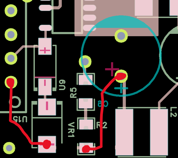
- Instead of connecting to the input inductor L2, the resistor R2 should be directly connected to the positive terminal of input capacitor C6. Please refer to the attached image for your reference (Connection of R2 and VR1).
- The same goes to the anode terminal of primary TVS diode VR1, it should be directly connected to pin 1 of the transformer. Please refer to the attached image for your reference (Connection of R2 and VR1).
- Reroute the trace that connects resistor R6 to pin 1 of the optocoupler. As advised previously, avoid routing a trace underneath the optocoupler. Since the layout now uses 2 layers, you can use vias and the other layer to connect resistor R6 and pin 1 of the optocoupler smoothly. Please refer to the attached image for your reference (Connection of R6 to pin 1 of optocoupler).
After applying the changes, you may proceed with board fabrication and testing. I would appreciate it if you could provide the results of the new board testing once available.
Thank you and I wish you a great day and a nice weekend ahead!
Best regards,
Tommy
| Attachment | 大小 |
|---|---|
| Connection of R2 and VR1.png (90.98 KB) | 90.98 KB |
| Connection of R6 to pin 1 of optocoupler.png (68.4 KB) | 68.4 KB |
Hello TOMMY BRADFORD
I am back after a few months. We have fabricated our new board using the TNY286DG-TL, and I tested it with a 250mA load. With our new design, we have exceeded its power rating, and now I am testing it with a 250mA load at 5.5V. Our new board delivers 250mA, but the issue is that the load only operates correctly when we power on the SMPS first and then apply the load. In other words, it works well during a late load test. However, if we restart the SMPS while the load is pre-attached, the voltage starts fluctuating, and the load begins to blink.
This is quite frustrating. Why is our SMPS not functioning properly?
I changed VR1 from P6SMB120A to SMBJ150A, but I can also test it with 1.5KE180A or P6KE200A if you believe the TVS diode is causing the issue. I also replaced C3 (470uF) with 1000uF and 220uF, but that did not solve the problem. Additionally, I changed the BPM capacitor from 10uF to 1uF, but that still did not resolve the issue.
Please review this situation once more, as it is causing us a lot of stress.
Thank you.
I attached the Gerber file, and pictures of the PCB board
| Attachment | 大小 |
|---|---|
| Gerber_PCB_Rev2_2_2026-04-17.zip (38.29 KB) | 38.29 KB |
| TNY286PCB_Pic1.jpeg (59.94 KB) | 59.94 KB |
| TNY286PCB_Pic2.jpeg (70.53 KB) | 70.53 KB |
I am sharing the PI expert-recommended design too.
| Attachment | 大小 |
|---|---|
| TinySwitch-4_PIDesign2_0.pdf (2.06 MB) | 2.06 MB |
One important point to note is that with the 470uF capacitor at C3, no components get hot; however, the 1000uF capacitor makes the TNY286 hot, along with some other components.
I apologize for not mentioning earlier that I achieved a 5.5V output by using a 12.1K and a 10K resistor. I wanted to update you that I am currently testing a load with a PCB board that has two resistors in parallel, each with three LEDs that are also connected in parallel. Let me share the schematic of my test board with you.![]()
Does this test circuit board cause any issues with my SMPS? I'm asking because I have tested it with a Nextion HMI, which works as expected. When I connect the Nextion HMI as a load, it makes my SMPS output 5.44V and draw 0.23 Amps of current. At no load, I get an exact output of 5.52V.
This is a picture of my load test board schematic
| Attachment | 大小 |
|---|---|
| load_board.png (44.55 KB) | 44.55 KB |
Before the end of the day, we will replace the transformer with a sample from another vendor, which should make our SMPS work properly. I will conduct further tests and share the results with you.
I have tested my two parallel assembled boards to increase the current, and the SMPS is delivering 0.53 amps at 5.51 volts, which is great. I also tested my Nextion HMI, and our SMPS provides 0.23 amps at 5.51 volts, which is good.
No components have gotten unusually hot. I will test with a 1 amp load and let you know the results.
Hello Ahtisham@Enfana,
Good day and I hope you're doing well.
Based on my understanding, the current problem you're experiencing with the prototype board is that it cannot start up (triggering the auto-restart) when the load is connected (startup full load). Can you clarify at which input condition you encounter this issue?
First, please double-check all the diodes and optocoupler to see if they are soldered in the correct orientation and if all the values of each component are correct. Since the design is also in an INCREASED CURRENT LIMIT configuration, kindly keep the value of the BPM capacitor (C7) equal to 10 uF. The voltage rating of VR1 is also too low relative to the transformer's set reflected output voltage (VOR). Since the VOR set was 135 V, its breakdown voltage rating should be around 170 V and above to prevent excessive heating during normal operation.
If all component values and their orientation are okay, then I highly suggest probing the drain-source voltage of the TinySwitch-4 together with the output voltage using an oscilloscope to verify if the device is properly switching and if the output voltage is reaching regulation within the auto-restart on time (64 ms).
If we can confirm that the output voltage is not reaching regulation within 64 ms, can you try reducing the value of the compensation capacitor (C8) that is connected between the cathode and reference pin of the TL431? A value of 100 nF might be too high, causing the output voltage to have a slow startup. A good starting value for the compensation capacitor would be between 10 nF and 22 nF.
Then, based on the latest PI Expert file you've shared, I noticed that a warning was flagged mentioning that the "maximum duty cycle exceeds device limit". This warning might also result in start up issue during full load condition (1.5 A) at 85 VAC input. Below are two options you can implement.
- An easy fix for this is to increase the input capacitance value significantly to increase the effective minimum DC input voltage. Changing the value of C1 from 10 uF to 18 uF is suggested.
- If you want to keep the same size of input capacitors (and their values), another recommended solution is to decrease the reflected output voltage (VOR) of the design. This will update the number of turns of the transformer construction. Please refer to pages 7-8 of the attached PI Expert file for the new transformer. construction.
I hope that the information above helps. Feel free to reach out again if there's anything else that I can help you with or if you have any further questions or clarifications.
Thank you and I wish you a great day ahead!
Best regards,
Tommy
| Attachment | 大小 |
|---|---|
| TinySwitch-4_5.5V_1.5A.pdf (2.06 MB) | 2.06 MB |
Hello Ahtisham@Enfana,
Good day and thank you for choosing Power Integrations.
I'm sorry to hear that you're experiencing this type of issue. I would really appreciate it if you could also share the actual PI Expert file (in PDF format) of this design, the transformer datasheet from your transformer manufacturer, and the PCB layout (Gerber files preferred) so we can review further.
Now, since the issue is related to the output voltage regulation, could you try decreasing the value of resistor R6 (in your actual schematic) from 500 ohms to around 47 ohms and check if there will be any improvement in the regulation of the design? The current 500 ohms value is too high for the design preventing the optocoupler to transfer enough current to pull low the EN/UV. Additionally, I also recommend connecting a 1 kΩ resistor in parallel with the LED part of the optocoupler because it sets the minimum operating current for the TL431 at approximately 1 mA.
You can refer to the attached image for the typical component values of the feedback section when using TL431.
Please let me know if the recommendations above help resolve your issue.
Thank you and looking forward to your response.
Best regards,
Tommy