
Radiation emission failing in TOP267KG-TL based SMPS
I am using TOP267KG-TL for 4.5 W output. At 19.2V DC converter operating in CCM, But from from 40V above it is operating in DCM.
Input: 19.2 - 373V DC & Universal AC input
output: 12V, 4.5W
Transformer: Primary 24; Secondary 15; Auxiliary 16 ( output voltage 15); Primary magnetizing inductance 280uH, Leakage 5uH
TOP267KG-TL: 1) V pin is shorted 2) At X pin & ground 16K resistor connected
Results: Converter is working fine in entire AC/DC input voltage range. Functional testing is fine.
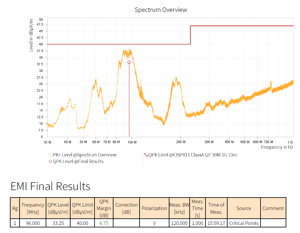
Problem : It is not passing with RE test (CISPR11 Class A).
- Currently we are getting best results (4-4.5dB) with RCD snubber( 2.2nF, 45.5K, US2KA, 22R damping resistor) & RC(442R, 94pF) across top switch. RE result is attached ['RE_result_4.2dB' file]. Secondary side no snubber. WE need margin upto 8-10db.
- If we follow point 1 and add 1nF Y cap across positive primary DC link to secondary ground, Then we are passing with 6-7 dB margin. But with this Y cap, we have problem in other tests. So, We can't keep Y cap. We need find alternate solution? (file- RE_result_with Y cap C1)
- Along with point 1, we tried with different combination
- Snubber across secondary - not helping
- In secondary currently using ES3G-E3/57T( general purpose ultra fast diode 35nS). we changed to schottky diode - not helping
- In RCD snubber, R & C values changed - not helping
- In RCD snubber, US2KA(trr 75nS) diode used. This diode changed to trr 35nS diode & trr 150nS diode - not helping
- In RC snubber across top switch, R vaules changed 300R, 663R - not helping
Any other suggestion to improve this RE results?
Please tell which area has to be targeted?
Comments
Hello Mayur@111,
Good day and thank you for choosing Power Integrations. I really appreciate your detailed summary of changes.
One of the key factors affecting EMI is the PCB layout, so it would be really helpful if you could share the PCB layout (Gerber files are preferred) and the schematic diagram with us. This way, we can take a look and offer suggestions to further improve the radiated EMI performance.
For the time being, you can read through the attached file (AN-15) for the TOPSwitch® Power Supply Design Techniques for EMI and Safety. It is mentioned on pages 23 and 24 how they reduced radiated emissions.
Looking forward to your response and the requested files. I wish you a great day ahead.
Regards,
Tommy
| Attachment | Size |
|---|---|
| an15 - Power Supply Design Techniques for EMI and Safety_0.pdf (462.19 KB) | 462.19 KB |
Hi good morning PI team,
I am waiting for your response.
Regards,
Mayur