
Optocoupler LED resistor discrepency
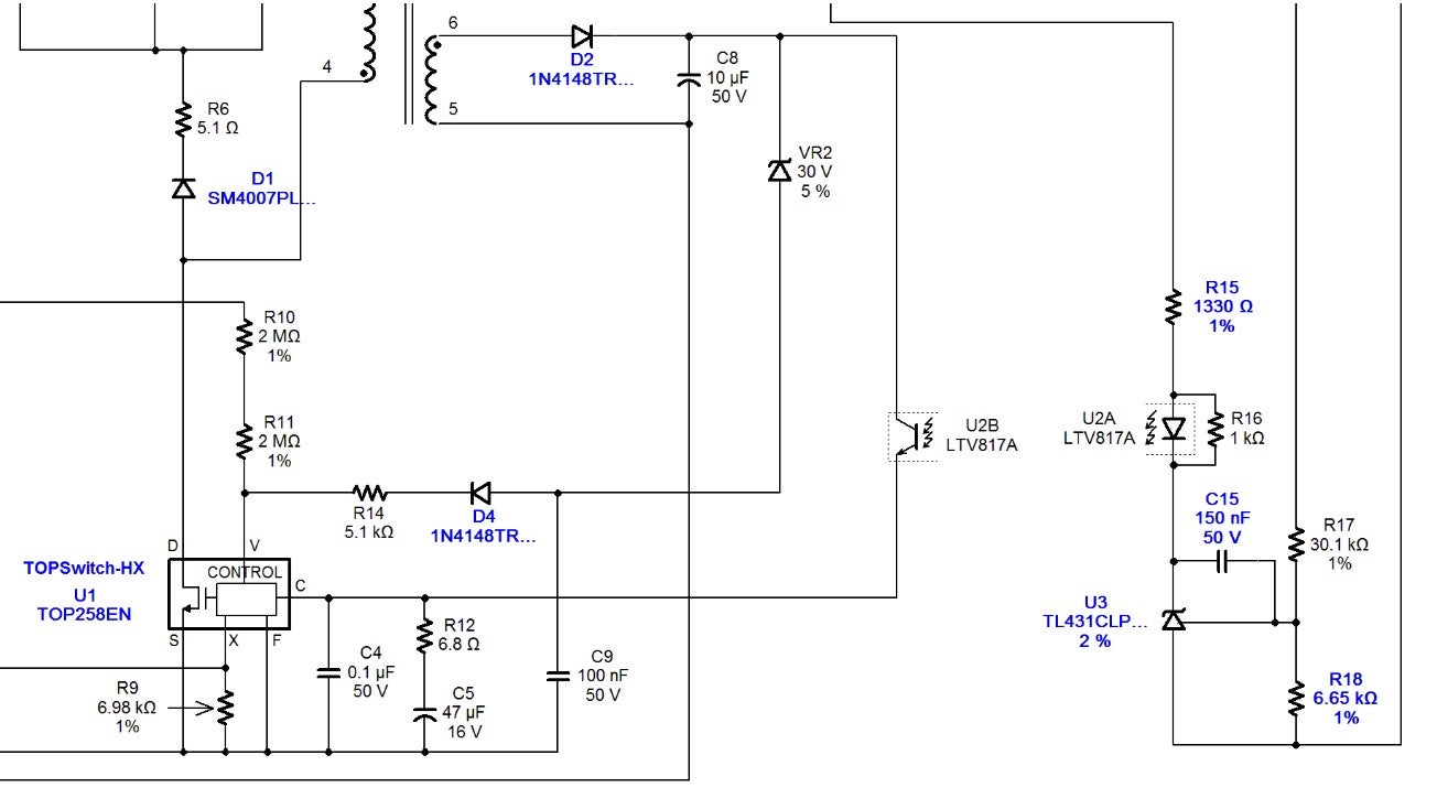
I made a 13.8V, 8.4A AC-DC power supply using PI Expert Online. The PI device used was TOP258EN. The suite suggested a 590Ω resistor for the optocoupler LED. This would result in a current of 23mA through input LED which would result in 37mA through output of opto.
The largest value I could select for the given design without an error was 1330Ω. This would result in at least 10mA flowing through the opto input. Which would result in a current of 16mA flowing through the output of the opto.
Both the values were verified on the physical prototype by disconnecting the output side of the optocoupler and measuring the current flow with different resistor values for the input LED.
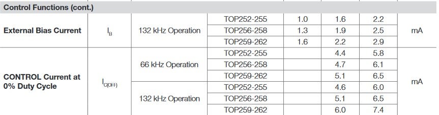
However, in the datasheet for TOPSwitch HX series convertors, the Control pin current for 132KHz operation is specified as 1.9mA typical and 2.5mA Max. The absolute maximum is 100mA and well withing the maximum current through the opto(50mA). The CONTROL Current at 0% Duty Cycle or IC(OFF) for TOP258 at 132KHz is 5.1mA typical and 6.5mA Max.
My convertor is not producing any output and seems to be stuck at soft start. I was wondering if the current outputted by the opto must be stopping the device from powering up. Is there a chance for the IC to have been damaged by excessive current through control pin?
Attached:
1. PI Expert Suite snippet of the feedback circuit diagram
2. Datasheet snippet of ratings
3. Datasheet snippet of Control pin characteristics
Comments
I disconnected the output stage on my board from the transformer and powered it externally with the expected output voltage. The output part of the optocoupler was removed from the board and given a power externally. I did that to just check whether my feedback elements were functioning or not. TL431 is behaving as expected and the opto gets powered on when the reference value is met. Now I understand how the current through opto is not solely dependent on the resistor after reading your reply.
In the attached PCB Layout R17 is R17-3. The output after C17 has a fuse on each final output channel.
I made another design using TOP259 and the design suggested had no current limiting resistors. Everything else was similar to old TOP258 circuit ,ade by the suite. I emulated the same on my board by removing R7 and R8 and then bridging R9. TOP258 was replaced with TOP259. Gain adjusting resistor was changed to 1Kohm from 590ohms. Rest of the circuit was same as the old TOP258 prototype.
I will post the other waveforms you requested soon.
Please suggest a solution with TOP259 if it can be done on the existing layout.
Attached:
1. PIExpert Design file for TOP258
2. PCB Layout
3. PIExpert Design File for TOP259
4. Layout with Labels
| Attachment | Size |
|---|---|
| PIExpert Design file for TOP258 (2.39 MB) | 2.39 MB |
| PCB Layout (199.68 KB) | 199.68 KB |
| PIExpert Design File for TOP259 (1.42 MB) | 1.42 MB |
| Layout with Labels (192.38 KB) | 192.38 KB |
Hi,
I am not what are your safety requirements or surge specs, I saw that primary to secondary creepage distance is very less.
Please take a look at page no's 28-31 of the data sheet, it has recommended PCB Layouts.
I am also giving you a link for one of the design example which is the closest that I could found for your specifications. You can take this as reference and work on your design.
https://ac-dc.power.com/sites/default/files/PDFFiles/der218.pdf
Regards,
PI-NANO
Thanks for the design resources. I modified the layout accordingly.
Turns out that our transformer was not up to the specifications.
Hi,
I am not sure how you have calculated current flowing through the optocoupler LED, Generally current flowing through the Optocoupler LED is determined by TL431 Error amplifier output not the resistor so much. Resistor sets gain of the open loop transfer function.
For compensation design process please read through the following application note.
https://ac-dc.power.com/sites/default/files/product-docs/an57.pdf
As far as the problem with startup that you are encountering, Can you send me couple of waveform captures.
Primary Drain current, Control pin voltage, Output Voltage etc.
Also Can you send the complete PIExpert design file and PCB layout for this design as well.
Regards,
PI-NANO