
LNK625
Dear All
hi
greeting Morning
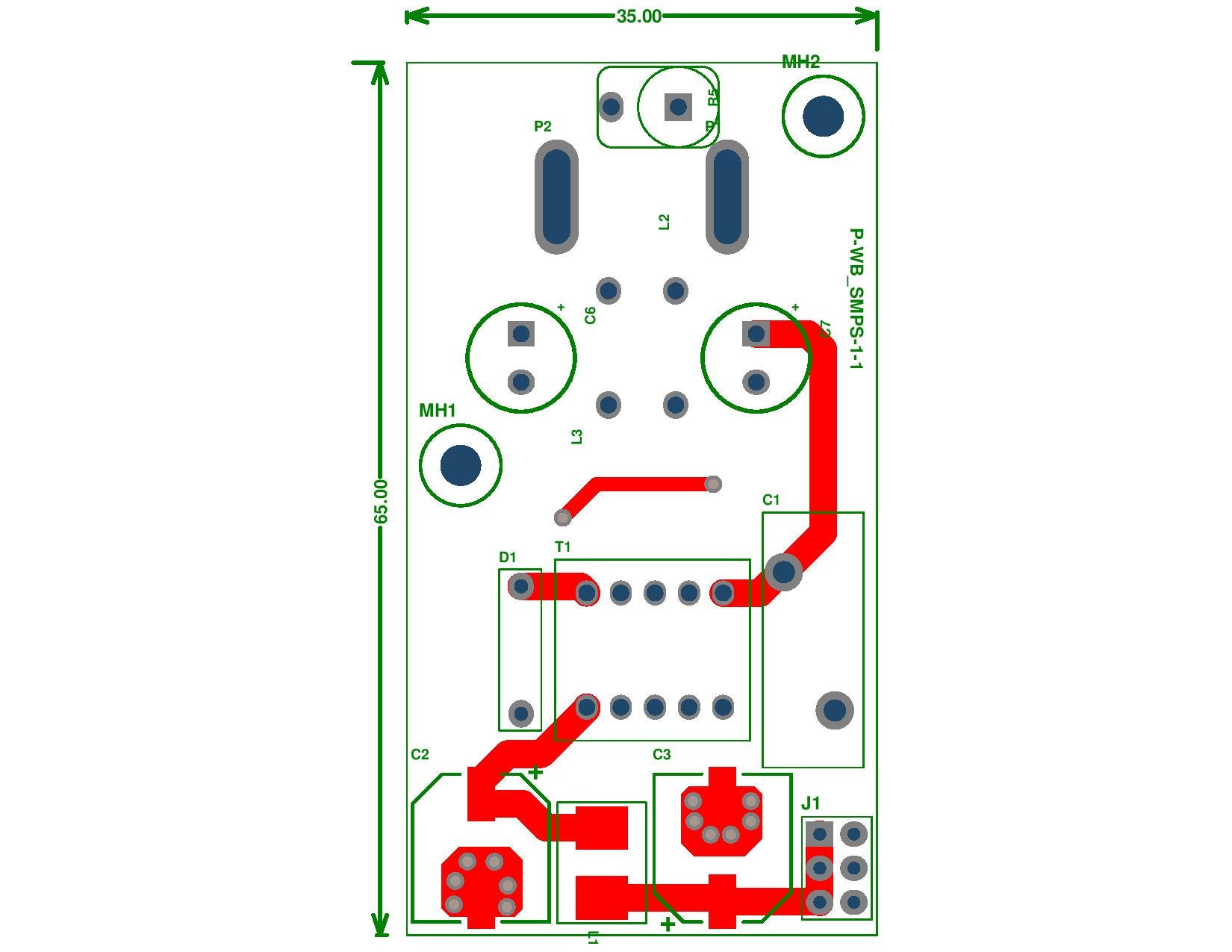
i am new in Power electronics Design.and this is my first SMPS Design with LNK625DG.I have Placement All Components as my best.
i have need Suggestion to make deisgn more Suseptible ,Less noisy ,Better EMC and EMI Design.
i have attached my schematic file and placement file.
please reveiw it and give your vluable feedback to me.
Best regads
Kamlesh patel
回應
Dear Sir
i have attached Jpeg File,please find attachment.
Please Notify me if possible as soon as possible ,because i have did line of project.
| Attachment | 大小 |
|---|---|
| Schematic of power board (110.24 KB) | 110.24 KB |
| Top side view/layout (122.75 KB) | 122.75 KB |
| Bootom side View/Layout (96.5 KB) | 96.5 KB |
Hi,
I think your layout seems fine. My only suggestion is that you may want to bring some of the input-side components closer to the right to make the board size smaller. Remember to minimize the primary-side loop components which would help with the EMI and to always consider functional isolation requirements (creepage and clearance) as well.
Regards,
Dear Sir
Greetings Morning
Thanks To reply.
we will work on your suggestion to minimize input side Loop.
Hi,
I can't seem to view the placement file you sent. Could you send a .jpg file instead?
First of all, welcome to the world of power electronics design. I can see that you are using a LinkSwitch-CV part in your design. To help you in your design iterations, you may use PI expert online (https://piexpertonline.power.com/site/login). In designing SMPS, there are numerous techniques with corresponding trade-offs. In flyback design, it would be best that you optimize the transformer first before proceeding with other techniques. Optimizing the transformer would be a good starting point; solving issues just with transformer construction can help you eliminate the need for additional components and other external fixes. You may want to consider adding a bias winding (to power the BP pin externally) shield and cancellation windings (for EMI improvements) and tweak the number of primary and secondary turns for improved efficiency.
In terms of layout and component placement, identify high dv/dt or switching loops and minimize these loops in the layout. Also consider the required safety isolation (creepage and clearance) for high voltage components.
As a reference, you may look into DI-201 (6W, 5V design: https://ac-dc.power.com/design-support/reference-designs/design-examples/di-201-6-w-high-efficiency-adapter-power/)
Regards,