
TNY278P STACKFET DESIGN BLOW OUT PROBLEM
Hello,
Please reply urgently,as it is very serious issue and we have very little time.
For one of our product, we have a Stackfet power supply with TNY278P, with following specs.,
Input- 3 Phase 150 to 450 VAC
Output- 14W Peak (7.5V,1.8A)
Normal Output Power- 6W, (7.5V, 0.8A)
Measured Efficiency- 70% Approx at 230VAC.
The SMPS blows out sometimes immediately after applying voltage, sometimes after few days on field or sometimes in a month or two.
Each product get damaged now or then.
The parts which get damaged are,
R17,18,19 -Inrush current limiting resistors (3W Wire wound)
Bridge rectifier diodes.
U4-TNY278P
Q3- MOSFET
D17- 15V Zener
D18- TVS Diode P4KE550A
R32-10 Ohm
I have attached Actual circuit with parts and value and PIXLS design file.
At first, we didn't use the inrush current limiting resistors and a Mosfet's 15v zener (D17), because the mosfet has its internal
Gate to source protection zener connected back to back two zeners as shown in mosfet datasheet.
As we encountered the burnouts we placed an external 15v zener, but still the problem didn't get solved.
Then, as there were no inrush limiting resistors, we felt that the rectifier diodes got damaged by high inrush current stress and then subsequently other parts got damaged,
So we placed three 47R 3W Wire wound resistors to each phase, but the sequence of burnouts continued including these resistors.
We also tried to increase PIV of input rectifier diodes buy placing two diodes in series for each leg making total 12 diodes, but the problem didn't solved.
then we also changed the supplier of TNY278P as we thought it might be a counterfeit part, but even then the burnouts continued.
When the SMPS works, it woks completely perfect with no heating, perfect load and line regulations.
We are in great trouble as we can't figure out which part/s gets damaged first and then others follow as its consequence.
Please help on this issue.
Thanks and regards.
SI.Tech
评论
The parts selected are abundant in ratings such as, 2000V,1A PIV rectifier,
600V,4A Mosfet, 200V TVS Snubber diode, 550V TVS device drain voltage clamp diode. So I don't think that any component is under stress.
Please clarify my few suspected doubts.
1)The transformer primary inductance in manufacturing goes upto 1.3mH (30%) against 1.015mH suggested by PiXLS.max tolerance suggested is (10%) in pixls.
2)The leakage inductance is 40-50uH against 30uH in pixls.
(Transformer inductance is adjusted by adding paper gap.)
3) Is P4KE550A with 550 V, too high to clamp TNY278's drain voltage to 700v ?
4) Does MOSFET's internal zener + added external 15v zener increase Gate charge? thus makeing it sluggish in fast switching?
Although the mosfet selected is fast enough. I have attached datasheet of mosfet.
Please check the datasheet of the mosfet if it is good for this application and power. also check other aspects of MOSFET such as avalanche rating, dv/dt, ON time OFF time etc.
5) Can minor voltage transients at input add a glitch to the operating of device and destroy any of the part? As there is no MOV placed at input section.
6) The power supply is designed for 14W but it mostly operates at 0.5W and occassionally upto 3-4 W. Can this be a problem?
7) Can PCB layout be responsible for the failures?
| Attachment | 大小 |
|---|---|
| stp4nk60z.pdf (701.33 KB) | 701.33 KB |
1. 30% is very high. If pixls suggested 10% then this is the maximum inductance that can be used without having the transformer saturate specially at high temperature. Most TRF manufacturers can meet 5% tolerance.
2.Leackage inductance can cause very high voltage spike across the switch and may destroy it.
You can decrease this by sandwiching secondary in primary halves.
3.This should be ok since stackfet.
4.No. This should only act as an over voltage protection on to the gate.
5.Yes. that is why I asked you measure all stress on all devices as this should be standard.
Start-up/normal operation, lowline/highline, full/no load conditions and should be on proper derating (ex FET 90% max voltage on VDS) in the long run you would see field returns if you don't ensure this.
6.No
7.Sometimes if you don't ensure proper PCB track clearances with respect to voltage levels.
Regards
Hii Data,
Thanks for your comments.
1) For 440VAc system, my minimum track clearance is 3mm. Is it ok?
2) Explain me in detail how higher primary inductance can blow my design apart from the fact that the transformer saturates by higher inductance.
3) Also explain that how higher leakage inductance can blow the SMPS without damaging the snubber diodes. (because in my design snubber diodes dont get damaged). Explain this too in detail please.
4)Also, i think input transients is not the problem because we now had used MOV of 510VAC and still it blow. Now only rectifier diodes and Inrush current resistors get damaged.
1.3mm is ok.
2.I did not say that it blow your design but it may lead to.
What I am saying on this is you should not be operating your design in saturation.
As we know if the TRF saturates primary current will have higher peak current than usual and may cause current/thermal runaway and could could lead to other instability.
3.This leakage inductance causes spikes on primary switch and snubber diodes are just their to dump the spikes. This spikes is present only when the snubber diode is conducting so it only act as a short circuit and won't be able to damage.
4. I am not sure what do you mean here..
I mean,
We thought that transients coming from line could be damaging the parts, so we placed 3 Varistors of 510VAC each just after the input resistors to block surge and transients. That means now no surge over voltage and transients appear at input.
But still the Inrush resistors get blown as a consequence of shorted diodes, other all components are ok.
One thing i have noticed is that only lower 3 diodes get short circuited. The upper three are fine.
How could the lower rectifier diodes be damaging? Which rating of diodes might be exceeding, the current or PIV?
If lot of current is flowing through the diodes, so should it flow through mosfet and TNY and they should also get damaged, but they don't.
Also have a look at the other circuit shown below the smps circuit, if does it play any role in damaging the diodes? This is a frequency detection circuit and is connected to input side of smps and fed to microcontroller after opto isolation.
Hi,
Can you check the Vds of the switch on Q3 and Tny and combination of the two at Max Vin and Full load. I am not sure if your snubber with a diode and a TVS is enough.
Regards.
OK, I will check.
1) by the mean time, tell me that in my PIXLS file, CMA(cmils/amp) is 999. And recommended CMA is between 200 and 500.
Is it a obvious big problem?
I am attaching pixls design file.
2)How to check drain current waveform?
| Attachment | 大小 |
|---|---|
| GSMST_7.5V_1.8A.pixls (48 KB) | 48 KB |
1)300 CMA-500 is the optimum
2) You have to cut trace and add a small wire for current probe.
Regards.
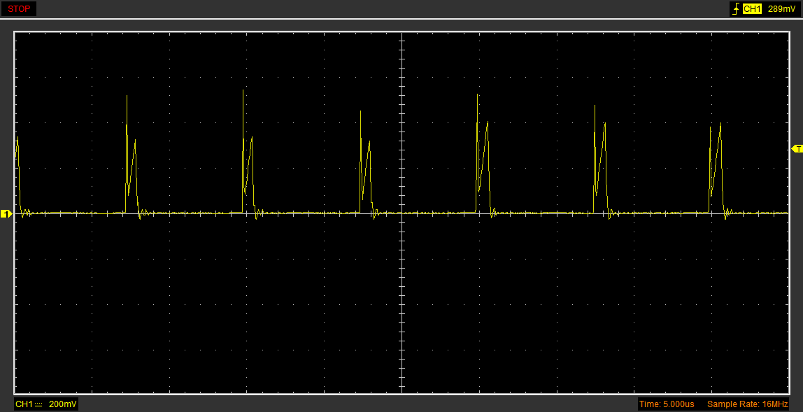
Hello,
Attached are the Voltage waveforms captured across transformer, and Drain current waveform.
Few things i noticed
1)Why is there a spike in current waveform at the beginning? Is it normal? I thought it is due to secondary rectifier hence i replaced it with fast reverse recovery schottky diode, but the the spike didn't go away.
2)In voltage waveform why there are 4-5 Sine wave like valleys? Sometimes only a half vally.. are those ok?
3) I noticed that most of the times the switching frequency is 66 Khz and not 132Khz as specified in datasheet.
Any clue?
| Attachment | 大小 |
|---|---|
| Voltage1.png (13.36 KB) | 13.36 KB |
| Voltage_240V.png (12.7 KB) | 12.7 KB |
| Idrain500vdc.png (10.73 KB) | 10.73 KB |
| Idrain640vdc.png (10.01 KB) | 10.01 KB |
Hi,
Below response.
1.Spikes are normal at the beginning of the drain. The controller have blanking time at the beginning of the drain current so current limit won't be false triggered. This spikes are caused by leakage inductance of the transformer. Leakage inductance is usually acceptable at 3-5% of nominal inductance. Although you are correct to use schottky diode as ther are usually used for this type of application.
2. Yeah these are ok. Depending on the input voltage and output load, the duty cycle is varied that is why you are seeing deep DCM and critically DCM.
3.132KHz is the maximum switching freq capability of the IC. It won't necessarily reach 132KHz. Switching freq depends on input voltage and output load.
Regards
I know that the issue s probably solved since long time ago, but I'll post to be useful for other readers.
To me, the problem is absolutely obvious being due to parasitic spikes on the 400V 3-phase input.
In industrial environment, where big motors are switched on and off al the time, taht is a common issue.
Situation can be solved with MOV's, but these have to be very close to the TNY 700V limit, not over, and not too much under.
That mean 510Vac are far too high, the MOV's on each need to be 680Vdc [ !!! please ensure the marking on the MOV body is 681 !!! ]. And after that raise the value of input resistors (inrush) to at least 30 ohms or more, to not blow the fuses all the time.
I would also use ESD diodes at the top of the snubber, that mean from snubber V++ to GND, same voltage, 680V
Hi,
It is also important to note that you still don't know at what exact state or condition that it actually breakdown. From my point of view, if it is really working sometime then I think you have some reliability issues. Specifically stress on the components that causes components to fail. Some components may still works even it exceeds the rated voltage/current/power but it is not 100% all the time. What you can do is to measure voltage and current stress to all components most specially the active components.
Regards.