
query on design example suggested for TOP221P
the attached schematic was mentioned as a design example for TOP221P in page six of the datasheet . I had following queries on the design:
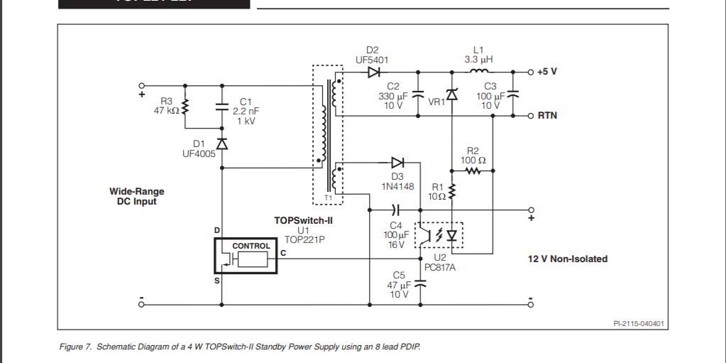
1. Its written in the datasheet that maximum rating of CONTROL pin voltage of the IC is 9V. But the design example gives 12 V to the CONTROL pin directly when the opto-transistor in U2 is on. Is this ok?
2. There is no discharge path for C4 in the design example. is it ok?
Please clarify.
Comments
Hi Prangyan15,
Thank you for your interest on PI product. As for your inquiry, kindly see below reply:
1. When the transistor is on, U2's collector current is U2's diode forward current multiplied by the CTR. This current is then feed to the Control pin via the voltage of C4. But the control pin have a shunt regulator internal to the chip, so the voltage there is not actually 12V but rather only around 5.7V.
2. The discharge path of C4 is the IC consumption. The IC shunt regulator (Control pin) is the one powering-up the IC and this is connected via C4. The C4 load is the IC itself. Thank you.
Best Regards,
PI-SevenofNine
Thanks for the detailed info:)
Hi Prangyan15,
Thank you for your interest on PI product. As for your inquiry, kindly see below reply:
1. When the transistor is on, U2's collector current is U2's diode forward current multiplied by the CTR. This current is then feed to the Control pin via the voltage of C4. But the control pin have a shunt regulator internal to the chip, so the voltage there is not actually 12V but rather only around 5.7V.
2. The discharge path of C4 is the IC consumption. The IC shunt regulator (Control pin) is the one powering-up the IC and this is connected via C4. The C4 load is the IC itself. Thank you.
Best Regards,
PI-SevenofNine