
Solid Copper on both faces
Hello.
I have 3 products, using the same power supply design.
Input: Universal AC
Output: 3.3 Voltios at 300 mA
Non isolated, with LNK306
Only one of them is working properly. the other two has over heating problems. so after a while the powe supply turn off.
I have checked everything: Connections, Voltages, etc. and everything looks good.
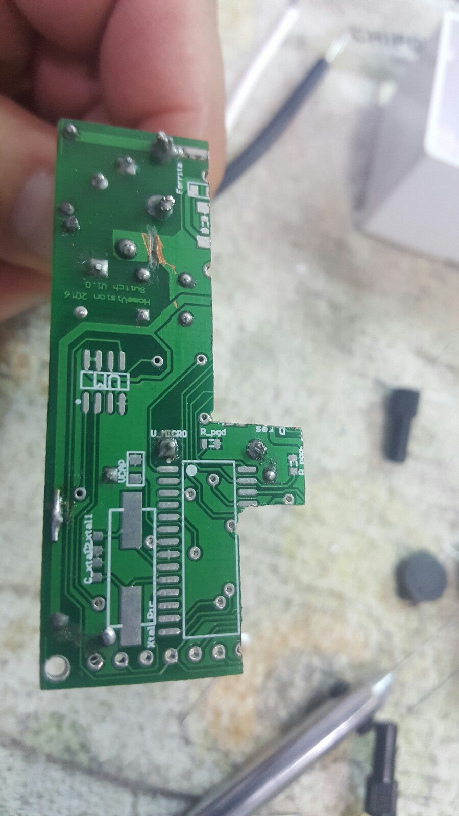
The only difference I can see is the two problems products have more solid copper connected to ground on both layers.
Is there any consideration when you are working on 2 layers PCB, when you pour solid copper on both layers connected to ground?
This is very anoying.
thanks.
Comments
Hi. Thank you so much for the response. I appreciate so much this help, since we wan to start production of those products as soon as posible.
I attached three .zip files:
Dimmer_1.zip are the gerber files for the product is working properly
Switch.zip are the gerber files for the product is NOT working properly
Shutter.zip are the gerber files for the product is NOT working properly
I attatched this file too:
Switch_OLD.zip are the gerber files for the previous version of the Switch product. and is still working properly
The changes in the new Switch:
- Filters and decupling capacitors for the Microcontroller
- Change of the paths of the NO, and NC pins of the rely.
- Change of the Resistor and capacitor position (the snubber connected at the output of the Relay)
I was making some test to the PCB of the switch, this weekend:
- I soldered only the power supply components (13 components)
- Power up the board and connected a relay test of 22.2 Ohmios, at the output: The Vout = 3.27 Voltios.
- After less 1 minute the temperature on LNK306 rise 40 degrees (in the dimmer product, with the same relay, the maximum temperature is 36 degrees, and take 10 minutes to rise this temperature. The same with the old version of the Switch)
- Since I cannot see any bad connection, I stared to cut pieces of the board. right now I have the minimum size of the board with the power supply componets.
- Make test again with the relay, and the PCB is still overheating.
- Start removing ground copper around the Neutral Wire,
- Make test again with the relay test. is still overheating, but it looks like takes more time to get 40 degrees.
I was making this test, since the only difference between the three PCB's (beside the paths of the connections), is the distance of the neutral wire to the ground copper.
Well, any help to solve this problem will be appreciate.
Bye.
| Attachment | Size |
|---|---|
| Dimmer Product New Version, Working Properly (45.48 KB) | 45.48 KB |
| Shutter Product, New Version, NOT Working properly (36.26 KB) | 36.26 KB |
| Switch Product, New Version, NOT Working Properly (34.66 KB) | 34.66 KB |
| Switch Product, Old Version, Is Still Working Properly (30.84 KB) | 30.84 KB |
Hi.
I forgot to attached the schematic,So sorry.
I guess this is the reason nobody has pay attention to my case.
As you can see I have two Zener in the design, one is TH and the other one is SMD.
I am using the TH only.
I would like to understand the problem, to avoid it in future.
Thanks.
| Attachment | Size |
|---|---|
| PS.jpg (34.56 KB) | 34.56 KB |
Hello cmlopez48,
Thank you for the schematic and Layout file.
From the layout, it seems to be fine. Are the schematic(components) between the old switch and switch file exactly the same.
For the "switch" board which you mentioned it is hotter than the old switch board, is the IC hotter or the whole board hotter. If it is not the IC, which component or which part of the board get hotter. When the board get hotter after 1mins, is the output still 3.3V? I am thinking if it is the IC get hotter, it means the IC is delivering more power and the power needs to dissipate somewhere. I am wondering if the output voltage increase or not.
By the way, for the output sense circuit, i notice it is am optocoupler and zener. we don't have any resistor to limit the current or bias the zener diode. Is there any difference between the sense circuit between the new and old board
Best Regards
Hi again.
Sorry for my late response, but I was making some test with interesting results.
The components are the same for the old version and the new version. Actually I bough a bunch of them, since I wanted to start a small production and test my devices in a real enviroment, not ni my lab. I have soldered 20 new dimmer PCB, with no problems. Around 5-7 new switch PCB, all of them with problems. And 5 new shutter PCB, all of them with problems.
The lnk3406 is the hot part, you get burn if you touch it, if the pcb has load.
As you say, the older switch board doesnt have the optocoupler, but I had some problems to get a stable output with load, so I modified the only one older switch PCB I have, and put the optocoupler. After this I got a better output with the load. I guess I posted that in the forum ,and you recommend me to use the optocoupler. To recap, the only one older switch PCB I have, has the optocoupler, soldering in not a fancy way. But is working properly.
Because of this, the new PCB design, has the optocoupler. I have 25 new dimmer PCB, 25 new switch PCB and 25
new shutter PCB.
Now, let me describe my tests:
TEST A:
1) Solder only the components related to the UPS, in the new switch board.
2) Sense the temperature in the IC lnk3406. It can reach 70 degrees after a couple of hours.
3) Start cutting pieces of the PCB, and sense again the IC, I realized everytime I cut some part, the temperature was lower, but not enoguh.
4) When I get the minimum size of the PCB, I started to remove copper areas, the GND area. After several trial and error, I got the minimum PCB modified, with no problems of heating.
The pictures are Test_A1, Test_A2 y Test_A3. After 10 minutes with the load ( 3volts relay with 20 ohm coil ), the temperature is about 31 degrees. You can see a snatchop in the Test_A4.
TEST B:
1) I took another new switch PCB, and started to remove the copper area, (GDN area). I tried to remove the same are like the PB I use in the TEST A. I cannot do the same, since I need the entire PCB. But I tried to reply the same situation
2) I soldered the components only related to the power supply. the pictures Test_B1 and Test_B2 are the bottom and top layers, with the modifications.
3) I Conected the PCB to the energy, and the load. After 10 minutes, you can see the temperature in the Test_B3. is around 60 degrees.
But right now the temperature stop at 60 degrees.
4) I did the same with 5 PCB. The minimum temperature I got is 47 degrees. The maximum is 60 degrees.
5) I soldered the rest of the componentes, Micro, memory, capacitors, etc.. The temperature rise 5 degrees more.
6) I tried to do the same to the new shutter PCB, but I could not get good results.
Can I conclude there is a problem in the design?
| Attachment | Size |
|---|---|
| Cutting New Switch Board, Bottom. (381.13 KB) | 381.13 KB |
| Cutting New Switch Board, Top (216.21 KB) | 216.21 KB |
| Load connected to the cutting new switch board (217.05 KB) | 217.05 KB |
| Temperature in the cutting new switch board (972.37 KB) | 972.37 KB |
| Test_B1.jpg (323.27 KB) | 323.27 KB |
| Test_B2.jpg (307.76 KB) | 307.76 KB |
| Test_B3.jpg (4.48 MB) | 4.48 MB |
Hello cmlopez48,
Thank you for the detailed test procedure and explanation. It seems that the thermal is very sensitive to the layout(copper plain at the GND).
Before you cut the GND copper, test procedure A3, how much temperature you get? When you mentioned "cut some parts", do you means the parts apart from the power supply related to LNK306?
For the copper you cut, procedure A4, i noticed you cut the GND copper close to Neutral and one close to the diode, did you cut anything else?
By the way, do you have oscilloscope in your lab? If so, can I ask the waveform of Ids and Vds of LNK306 for the good and bad switch board. I want to check if the current shape is right or not for between the low temperature and high temperature board.
Can you share the datasheet of the Inductor you used, the 470uH, Ltyp in the schematic.
Best Regards
Since I need to re-disign those two PCB, I appreciate so much your help in this issue.
The new original switch PCB, with only the power supply components, without cutted part, no removed gnd copper areas, the temperature go beyond 70 degrees. After two days connected with the load, I guess the PCB reach the maximum temperature, because the LNK3406 turn off, I mean, no 3.3 Volts in the output.
When I said "I cut some parts" I refer to the board in the TEST_A. And yes, the parts I cutted, was parts no related with the power Supply.
The parts I removed in the PCB for the TEST_B was:
- GND Area close to the neutral wire, on both sides of the PCB
- GND Area close the S line connected to the Inductor, in the Bottom Layer
- GND Area clos to the Nuetral wire in the top Layer,
- GND Area under the Inductor.
I have an oscilloscope, I am going to take measures in the old switch , and in the new switch. I can take measure on the new dimmer too, since is working properly.
This is the link of the inductor I am Using:
https://www.digikey.com/product-detail/en/bourns-inc/SRR1005-471K/SRR1005-471KCT-ND/2127378
Well, Today I will take the measure.
Thanks again.
Hello cmlopez48,
You are welcome and I hope the new design will become better.
One comment about the inductor you used.The saturation current is 450mA and the current rating is 300mA. You output current is 300mA which is already reach the current rating of the inductor. The current limit of LNK306 is much higher than 450mA which means the peak current in the inductor will be higher than its saturation current. I am wondering if the inductor saturate in those hot designs.
If possible, i highly recommend you change the inductor to one which has a higher saturation current>650mA
Best Regards
I hope you can still follow this thread.
I make the design for 300mA, since the maximum current will be 200 mA (I guess 180 mA).
If I connect the relay test to the dimmer PCB (the good design), this board never get hot.
so, anyway, will be a good idea to change the inductor?
I took the measure you requested me, but only the voltage. The current probes for the oscilloscope are SO EXPENSIVE. the cheapest one is 700 USD.
The voltage measure is Vds. The number 1 or 2, at the end of the name of the file means the division time of the osscilloscope.
I took measures with load an no load, for both PCB the good one and the bad one. Plus I took meausures of the bad PCB when is really hot.
I will find the way to take the measure of the current. But you wrote Ids? you mean Id and Is?
thanks.
| Attachment | Size |
|---|---|
| Bad PCB when is hot (obviously when the relay test is connected) (81.21 KB) | 81.21 KB |
| BAD_PCB_HOT_Load2.JPG (82.17 KB) | 82.17 KB |
| Bad PCB with the load. I took the measure a few seconds after the relay test is connected. (79.57 KB) | 79.57 KB |
| BAD_PCB_Load2.JPG (82.95 KB) | 82.95 KB |
| the bad PCB, but with no load. no relay test connected. (79.76 KB) | 79.76 KB |
| BAD_PCB_No_Load2.JPG (84.12 KB) | 84.12 KB |
| teh good PCB with the load connected (80.1 KB) | 80.1 KB |
| GOOD_PCB_Load2.JPG (82.26 KB) | 82.26 KB |
| teh good PCB without the relay test (79.83 KB) | 79.83 KB |
| GOOD_PCB_No_Load2.JPG (83.7 KB) | 83.7 KB |
Hello cmlopez48,
Thank you for the detailed voltage waveform. It seems that the good and bad PCB voltage waveform are similar. I think the current waveform will make more sense as we can tell if the inductor is saturated or not from the current waveform shape. the current waveform i mentioned Ids is the current from the IC Drain to source pin. It is better to measure it from Drian side as the source is the internal ground of the IC, connect a probe there may introduce noise to the ground.
If you you don't have current probe, you can tried with bigger current rating inductor >650mA to see if this issue is removed or not. If the inductor is saturated, the problem should be eliminated by using the bigger current rating inductor. The physical size of the big current rating inductor may be bigger. For the test purpose, maybe you find a way to connect it and check the thermal. If it works, then you can think about the componnet selection and change layout.
Best Regards
Hello cmlopez48,
Thank you for interested in using Power Integrations products.
Before we dig in, can I ask for the layout for all those 3 PCBs, in this way, i can have a better understanding of your 2 layers PCB difference.
For LNK306 application, in the buck or buck-boost converter configuration, since the SOURCE pins in LinkSwitch-TN are switching nodes, the copper area connected to SOURCE should be minimized to minimize EMI within the thermal constraints of the design.
For your case, as you mentioned the boards have problem has more copper as heat sink at source pin. it should not casue over temperature issue as you have more heat sink. I am wondering if it is related to noise coupling from the swiching node at source pin as you have bigger copper there. If you can share the layout and schamtic, it will be more helpful to dig in.
Best Regards