

Facing problem in 24V/2A design
Hi,
i have desined one SMPS with universal input and fixed output of 24V/2A using PI expert.
As I have used exactly the same components recomended by the PI expert BOM still not getiing the output.
i have attached the schematic and waveforms of control IC.
コメント
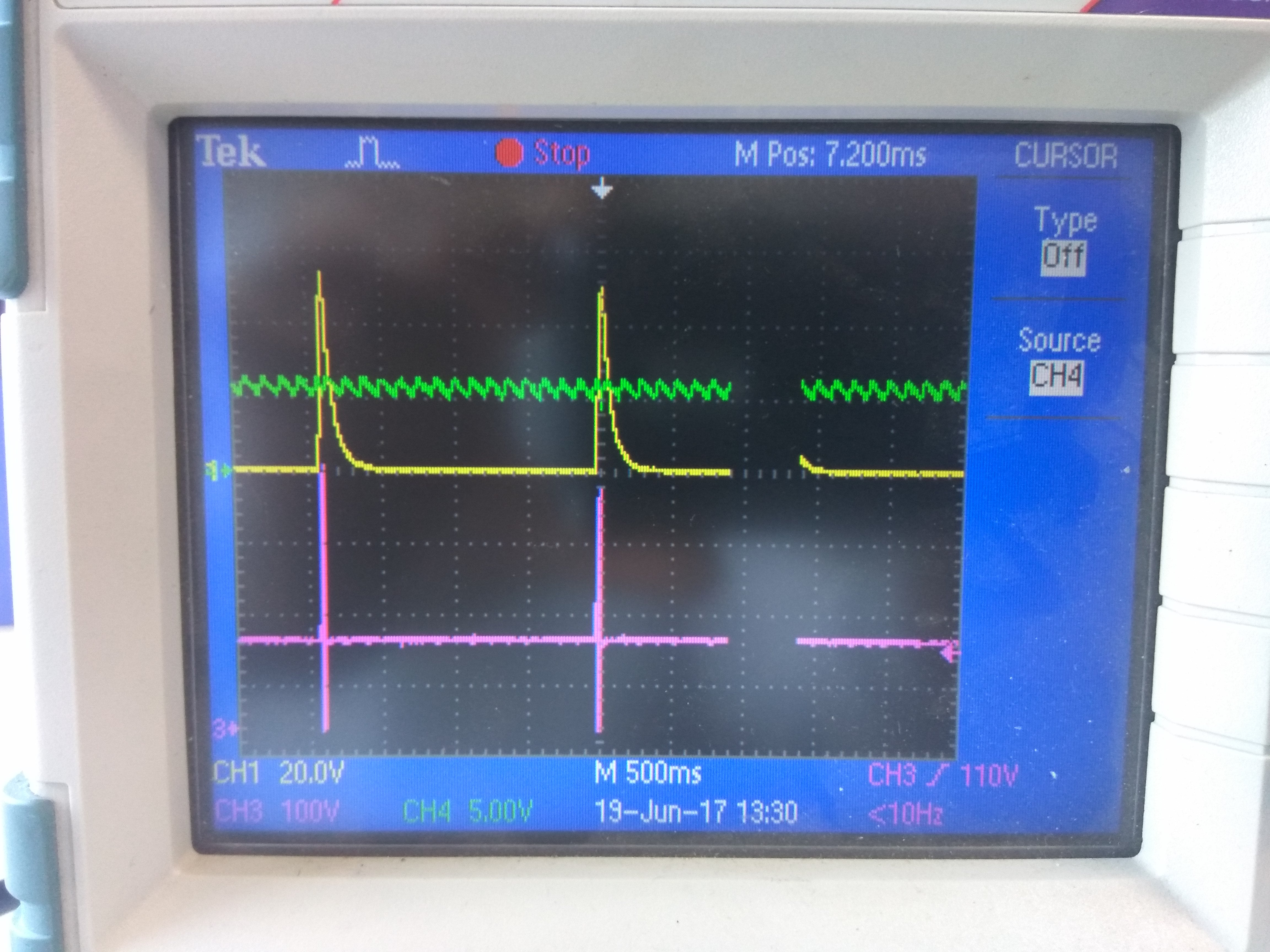
In waveform picture.
Yellow: it is the output waveform..where we expect pure DC 24V
Pink: it is the signal between drain and source.
Green: This the signal between COntrol pin of IC and source.
| Attachment | サイズ |
|---|---|
| Waveforms (1.97 MB) | 1.97 MB |
Hi Rohit Arora,
Thank you for using Power Integrations' part.
Regarding your question, my hypothesis is your transformer phasing connection. Your secondary winding should be out of phase from the primary winding and your feedback/bias winding should be in-phase with your secondary winding. You can try interchanging connection of your primary winding (pin 1 & 3), if not probably your your feedback/bias (pin 4 & 5). Transformer phasing is quite becoming tricky especially when you have more than 2 windings. Did you build your own transformer or it is off the shelf readily available part? Thank you.
Hi,
Thanks for your reply.
I build my own transformer as per the specifications given by PI expert.
I also thought in the beginning that polarity may be the problem, So i tried reversing the polarity of bias output and secondary output of transformer. But didn't help. I ask some of my colleagues, they are saying there may be some problem in the control loop.
I am not expert in this domain i have not changed anything in the control loop expect putting pot for R3 and R8 but it also didn't help.
Hi Rohit Arora,
Can you share the result of your PIExpert design? Did you follow the correct inductance value?
Your R8 value is too high. With your output voltage it should be around more or less 3K.
Hi,
I have attached the design file.
Please check and let me know what changes are required.
Hi Rohit Arora,
If you follow the schematic based on the PIExpert, I think the only problem you can encounter is with transformer. What is your measured transformer inductance?
Dear Mallora
Presently I was working with the Mr.Rohit project. Today I try to test it. But I have observed that output voltage is increase to 15V without the MOSFET switching. with some changes like I have removed the type -3 configuration(R9 & C12) and change to type-2 configuration. and added 500 ohm resistance between the cathode of TL431 and output. changed the clamping resistor R1 to 100K ohm. reduced the R8 resistance to 1Kohm.
I have measured the primary side inductance is 424uH.
| Attachment | サイズ |
|---|---|
| TOPSwitch-JX_PIDesign1.pdf (71.39 KB) | 71.39 KB |
Hi Gilla Bharath,
It is into auto restart mode. It pulses once i a while. Based on the previous waveform given, I think the Topswitch controller is not receiving feedback on control pin. There might some loop broken from the output going to C pin. You can check or replaced TL431 or the opto or any cold solder. Thank you.
Dear Mallora
Thanks, now I went for PCB. I have done the same as my proto test. But when I was testing on PCB. The Topswitch switch is resetting again at every 1.8sec. I have replaced all ICs near control circuit. Please help me in this regards. I have attached the waveforms. Yellow colour is rectifier bias winding voltage, blue is MOSFET across voltage & pink is DC link voltage.
| Attachment | サイズ |
|---|---|
| SCHEMATIC1 _ PAGE1.pdf (21.43 KB) | 21.43 KB |
| IMG_20171102_113955150_HDR.jpg (1.08 MB) | 1.08 MB |
Hi Gilla,
It seems your bias winding termination is not correct. Try to interchange pin 4 and pin 5 termination of TX1. I can't clearly see the timing between Mosfet switching and bias charge. The bias should charge once the mosfet turned off same thing with the output. Output voltage and bias should charge at the same time once the mosfet turned-off. If it is not correlated then there is wrong phase orientation. Can you provide voltage probe of the mosfet, bias and output voltage with clear transition so we can see that it has correct phase orientation. Are the C6, R6, R7 populated? Please remove that, it is not allowed on our products having snubber across the mosfet.
Dear Mallora
Thanks for replay. I haven't populated the C6,R6,R7. Please find the attached jpg file. It seems the polarity is correct.
Regards
Bharath Gilla
| Attachment | サイズ |
|---|---|
| IMG_20171103_085014299_HDR.jpg (977.71 KB) | 977.71 KB |
Dear Mallora
Still my board was not working. Can you help me in this regards.
Bharath Gilla
Hi Gilla,
Based on your shown waveform, The primary winding pin 1 and pin 3 should interchanged the termination. Based on your waveform, when mosfet is trying to turn-on, the output and bias is ramping at the same time. It should not be the case. See attached illustration of how it should switch for your reference. Please double check also the polarity of D2 and D3, make sure they have correct orientation in reference to your schematic.
| Attachment | サイズ |
|---|---|
| Mosfet_Vout_Vbias.png (19.29 KB) | 19.29 KB |
Hi Mallora,
Today I have populated the another board and checked the waveforms. Its working and I have captured the waveforms as attached. Its seems that the polarity is as per the specification only. But the output voltage is 35V. Please clarify following points
1) Polarity of transformer is correct or not.
2) MOSFET drian to source voltage going to negative voltage. why? is this due to snubber across MOSFET i have used(C6,R6,R7).
2) MOSFET spikes are too high for an input dc of 100V its voltage spike is of 250V. how to reduce it..?
3) Ring of the drain to source voltage is more, how to reduce it.
4) MOSFET is switching at 33KHZ. is it load dependent or not. As I have done with no load
5) Output voltage is going to 35 V instead of 24V. How to reduce it. I have tried to increase the resistance of led . But it is getting shut down.
5) if the polarity is correct, then what could be the problem in first board as i have used the similar components and board.
Regards
Bharath Gilla
| Attachment | サイズ |
|---|---|
| IMG_20171107_095403978_HDR.jpg (1.11 MB) | 1.11 MB |
| IMG_20171107_094852476_HDR.jpg (1.47 MB) | 1.47 MB |
| IMG_20171107_094936812.jpg (1.34 MB) | 1.34 MB |
Hi Gilla,
Good to hear your progress. Here are my answer/opinion on your questions.
1. Your waveform shows you have the correct polarity now. Maybe on your non working board, there is other ckt that is causing the mosfet current fault like wrong diode polarity on snubber ckt. It is hard to asses without checking the board by myself.
2. As I have said before, it is not recommended to use snubber across mosfet on our controller, you already have snubber at the drain to bulk to clam peak voltage due to leakage inductance. It should not have negative voltage between Drain and Source of u1, probably you are on AC Coupling setting.
3. What is your turns ratio between primary and secondary? Drain peak voltage = Input voltage + Reflected Voltage from the output which depends on turns ration + voltage due to leakage inductance (leakage depends on transformer construction and primary inductance value).
4. Yes it will vary with load.
5. Remove C6, R6 and R7, if it is still same output increase value of R20 or reduce R18/R19 until you got your desired regulation.
6. Same answer with number1. Check the difference between the board physically with parts orientations and values.
Hopefully it helps.
Hi Mallora,
Thanks for the answers. I have tried all the of reducing the R18/R19 resistor and also the increase of R20 resistor but it giving constant 45V output instead of 24V. please help me in this regards as my project getting delay.
Regards
Bharath Gilla
Hi Gilla,
Remove C15 and R17. Reduce C16 TO 33nF. Do you have pin 2 & 3 of J1 shorted? Try those and see if it will work. Thank you.
Hi Mallora
I have done the above test and I have observed that MOSFET is switching at 30khz instead of 66khz (when I have reduced the LED resistor to 3kohm my output is getting 24V but huge ringing) because of that my snubber is getting heated. when I was increasing the resistor value my output is going to 45V and MOSFET is switching at 66khz. Please help me in this regards as soon as possible.
Regards
Bharath Gilla
| Attachment | サイズ |
|---|---|
| IMG_20171208_091129360.jpg (1.48 MB) | 1.48 MB |
Hi Gilla,
What is the connection of your J1? Is pin2 shorted to pin1 or pin3? Please read specs of your controller from below link so you know what setting you want. Attached also is your schematic from PIExpert with the values, please check if you comply with this required connections and values. Thank you.
https://ac-dc.power.com/sites/default/files/product-docs/topswitch-jx_family_datasheet.pdf
| Attachment | サイズ |
|---|---|
| Topswitch_24V-2A_design.pdf (131.68 KB) | 131.68 KB |
Dear Mallora
Thanks for the replay. The problem was solved that was because of opto which has CTR of 80-600. Now I was trying to tune the output voltage. During the MOSFET turn on the output voltage is getting ringing of about 5V with 20MHZ. I have tried all the way of using filters and tuning the snubber circuit of primary transformer but it does not worked. I have attached the waveform for your reference . Please help me in this regards.
Regards
Bharath Gilla
| Attachment | サイズ |
|---|---|
| wave_form_during_MOSFET_turnon.jpg (1.03 MB) | 1.03 MB |
Dear Mallora
Problem was not solved still.Please help me in this regards. I was getting a voltage spike of around 5V at output with 20MHz frequency. the same spike is getting at output of auxiliary winding.
Regards
Bharath Gilla
| Attachment | サイズ |
|---|---|
| IMG_20180111_090507122.jpg (1.03 MB) | 1.03 MB |
Hi Bharath Gilla,
Try measuring the output ripple only, the other probes are possibly coupling on your ripple measurement. Then use a barrel or short loop on your probing with 0.1uF ceramic capacitor across. This is needed to eliminate coupled noise on your probing. Measure the ripple across your output capacitor. If your measured ripple is still not acceptable for you, try increasing ouput capacitance and using low ESR capacitors. Make sure you also have ceramic output caps. Thank you.
hi guys. i want design 24 v dc and 5 A out put. how i can computing Specifications of transformer?
thank you
Dear Mallora
I have conducted the RE test and it is failing. Please let me know the solution as soon as possible. I have attached the test results,sch, and Gerber file for your reference.Please help me in this regards.
| Attachment | サイズ |
|---|---|
| layout (53.95 KB) | 53.95 KB |
| SCHEMATIC1_03_POWER_SUPPLY.pdf (62.63 KB) | 62.63 KB |
| IMG_20180206_093419292.jpg (1.07 MB) | 1.07 MB |
Try moving C1, C5 to the left hand side of the common mode choke.
And, bigger snubber across D4 22pF is way too small...
and try 10E in series with C2 to dampen ringing on this part...
Hi Easy Peasy
I have done the changes as per above information but no changes in the results. I have already changed the snubber across the D4. I have used 681pf and 39 ohm resistor across it. voltage across the diode as shown in the attachment. I was observing a 1V of spikes at output as shown in the 2nd attachment. please help me in this regards.
Bharath Gilla
| Attachment | サイズ |
|---|---|
| IMG_20180222_154244513_HDR.jpg (1.12 MB) | 1.12 MB |
That waveform (on the o/p diode) looks OK, what are the remaining problems? ripple on the o/p voltage or something else?
OK, are C1, C5 now on the LHS of the CM choke? in any event they are too large for safety, 4n7 max, Y2 rated.
Also you need at least 100nF 250Vac across C3 to supply ripple current to the Tx, perhaps two in parallel. as all the RF noise is at the lower end of the spectrum - it could be DM rather than CM.
I have used 4n7cap with Y1 rated. sorry I forgot to change in schmatic. Ya they wer before the CM choke. what type of cap should I use across C3. is this an box type polypropylene cap like X cap...??
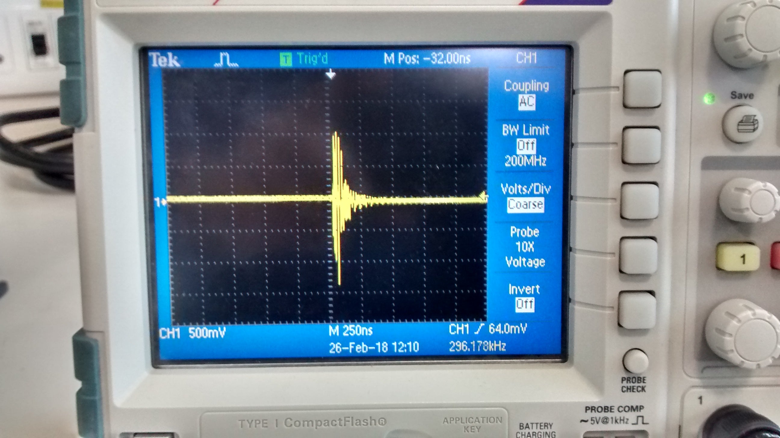
Spike at the output voltage as shown in the attachment was observed. frequency of ringing is 30MHz
| Attachment | サイズ |
|---|---|
| IMG_20180226_094509092_HDR.jpg (1.17 MB) | 1.17 MB |
OK, a lot of that signal is CM pickup, short your scope probe and touch it to the same point (Vo) do you see the same noise?
It appears you will need a more agressive snubber on the pri side too. C4 ->22nF,
or, even more cap on the diode snubber C6 (double it) and lower the R to 100E (R4)
Also the FR106 D3 is too slow, try a much faster type. C10 should be 1uF, or several in parallel
1)OK, a lot of that signal is CM pickup, short your scope probe and touch it to the same point (Vo) do you see the same noise?.....
Ans: Yes the noise is same as that of the attachment I have shared.
2) It appears you will need a more agressive snubber on the pri side too. C4 ->22nF,
Ans: I have parallel three 6.8nf but the noise is still present.
3) Also the FR106 D3 is too slow, try a much faster type
Ans: I have already tried with UF4007 and presently using same.
4) C10 should be 1uF, or several in parallel
Ans: I have placed the 1nF,10nF & 100nF already
C10 -> 1.0uF not 100nF or less
As your scope is picking up CM noise at an arbitrary level - you cannot really see what is going on - a big problem.
What is your main concern? conducted RFI? do you have a LISN and spec ann?
C10 -> 1.0uF not 100nF or less
I have place the same but no improvement..
when I was testing the standard module it is not showing any noise...
Presently I dont have LISN and spec ann.. The result which I have shared earlier is when I was testing radiated emission in LAB..
I have to visit the lab in next week.
you can also try CM cap on the output to earth, 100nF say, short leads. Radiated testing is very dependent on lead layout.



SChematic