
WHY a TOP266EG or TOP269EG explodes?
I have designed a 2.5A 24V output PS using PI expert and created several prototypes. I have used TOP266EG and TOP269EG as the controller. Some of the prototypes work without a problem. Some of them not. The difference is in the transformer. I have 4 different transformers. Actually they intended to be same. But three different people wound them. When measured with an LCR meter they have slight variances. 2 of them works without problem. But 2 of them does not. I mean when I inserted them into the circuit, sometimes the PS starts and works and sometimes TOPswitch explodes. Approximately 10 parts exploded while we try under both loaded but mostly unloaded condition. While some others works in all situations at full power for a long period of time. I don't know where to start to the inspection and where to look at. I only assume high peak voltage between drain and source but I could not catch such an event on scope so far! Please give me some ideas, thanks!
Comments
I have tried 4 different transformers with 2 different boards and made a table and attached it. You can check it.
I have also uploaded pi expert design file which I followed strictly.
What I really wonder, beside it's not working is, what causes the explotion and how can I prevent it?
Thanks.
| Attachment | Size |
|---|---|
| pi expert design file (368.5 KB) | 368.5 KB |
| Transformer test results (27.37 KB) | 27.37 KB |
Are there any opinions I need to conclude this quickly I don't have much time. I need to know why a PI part explodes to prevent it before an unpleasent situation occurs.
By the way it exploded once before when the leg of the optocoupler in the feedback path broken. Can it be related to feedback problem? Does not this part contain some kind of limitation to prevent part damage? Can transformer saturation cause this problem?
Have you checked that the winding polarities are correct?
When you are doing the tests are all windings connected? No winding should be left open circuit.
Winding polarities are correct. I made the measurements of winding inductances while all other windings are open.
Should I short all windings?
I've updated the test and attached...
attachment
| Attachment | Size |
|---|---|
| transformer test with windings open and shorted (31.83 KB) | 31.83 KB |
I did not satisfy with the leakage inductances and made the measurement with different lcr meter. Results are attached.
| Attachment | Size |
|---|---|
| Transformer test_diff_lcrmeter.pdf (33.2 KB) | 33.2 KB |
Your primary leakage inductance seems quite high at over 10% of the magnetizing inductance. At maximum peak primary current you will need to be dissipating approximately 7-12W in the snubber resistor otherwise things will start overheating/exploding. Your design file says that the snubber resistor only needs to be rated for 2W but this is for the required 1.5% leakage that the design suggests. I'm surprised the TOPswitch is exploding and not the TVS diode.
I was once told to aim for 5% leakage, which will approximately require 5W dissipation with your 150uH primary. This should be manageable with 1 or 2 resistors of reasonable size.
Research how to reduce leakage inductance and try winding some new transformers.
Thank you very much for the tips. I got it. Besides transformer construction, can you suggest any other measures that I can take in order to prevent or reduce component failures? Thanks again!
Hi,
Transformer leakage inductance is very high and it seems to be even higher with Transformer 1 and 2. When leakage inductance is this high, Vds might be exceeding it's breakdown voltagee. I think that is the reason for failre.
I saw that your design is single output design and split winding construction, so depending the type of bobbin that you use, you should achieve leakage inductnace between 1% to 3%.
Regards,
PI-NANO
One important factor I eventually found out that reduces leakage inductance is the coverage of the winding area on the bobbin. Winding layers should cover as much of the winding area as possible. Even if there are only a few turns on a winding it must be spread evenly across the winding area.
This is very relevant to real-world transformer design where enamelled copper wire will be used instead of copper tape. Who can afford to use copper tape like PI Expert always suggests? Most transformer manufacturers will charge the earth for copper tape, especially if they don't stock it.
Thanks I get the idea and that makes sense but I have still some confusion. My friend wound another transformer with much worse leakage inductance but be able to make it work by increasing secondary turns number and decreasing the value of the series resistor connected to the primary side of the (diode) opto-coupler. I think this arrangement forces the device to enter the variable frequency and variable duty cycle mode much quickly and easier and it prevents top26x to malfunction and make it works normally under light and heavy load. DC bus is ~330V by the way. Do you have any comment on this? I also wonder why snubber and transzorb does not protect the PI part? Thanks.
You are most probably right because I zeroed the airgap and there was still 7 µH leakage inductance...
I've added two waveforms about drain voltage at 70VAc and 220VAC inputs. Peak drain voltages seems to be equal!
| Attachment | Size |
|---|---|
| 70VAC Input.jpg (727.78 KB) | 727.78 KB |
| 220VAC Input.jpg (632.65 KB) | 632.65 KB |
What is your snubber resistor value? What diode are you actually using in the RCD snubber?
I have connected two 2W 47K in parallel and used MUR180 as a diode with a series resistor of 5.1ohms
I inserted transformer 2 into the circuit and first tried under 70VAC input under no-load and %15 loaded condition.
I turned power on- and off and on... and it worked well. I then increased input voltage gradually to 260VAC.
At that voltage without load it worked again but when I connected I load and applied the input power topswitch exploded again.
Does this snubber insufficient?
By the way transformer 3 had no problem under similar conditions.
I also want to mention I've made leakage inductance measurements at 1KHz. When I increase the test frequency leakage inductance decreases as frequency increases. It even turn to negative value at higher frequencies like 100 KHz that I don't understand...
Hi for no reason my account was BANNED! Perhaps actually helping people is prohibited on this forum.
Your snubber clamping voltage looks too low (~420V) from your photos. It looks like your turns ratio is about 4:1 and so is reflecting 100V (24V*4). At 260VAC the bus voltage will be about 367VDC, add the reflected flyback voltage this will be 467VDC. Maybe the power from the transformer is being diverted into the snubber.
Raise your snubber resistance and voltage/power rating accordingly so that the clamping voltage is above 467V.
Would that help this explosion matter?
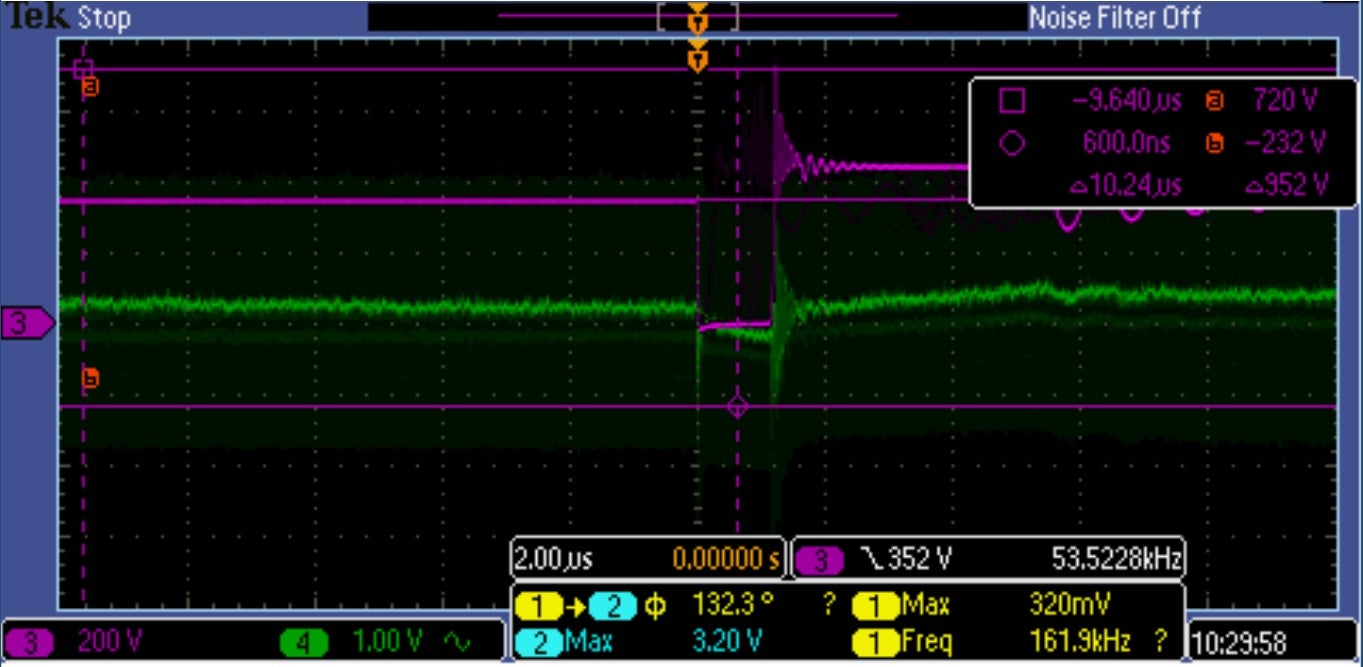
I realized that my differential probe does not work correctly and obtained two other differantial probes and saw that the problem really is the Drain voltage.
I also noticed that my previous TVS already blown and was not working. I replaced with a new one
and recorded a new image. The purple signal is the voltage between the dc bus positive and the drain, the green one is between anode and cathode of the TVS.
| Attachment | Size |
|---|---|
| 110V AC Input.jpg (600.27 KB) | 600.27 KB |
Sorry, the image is not clear and can't see a green trace
The direct line in the middle is ch4 and is green. at x100 scale it seems a direct line. There are 2-3Vpkk variations on it. I can send clearer images tomorrow.
Could you do some new Drain-Source waveforms?
First thing in the morning
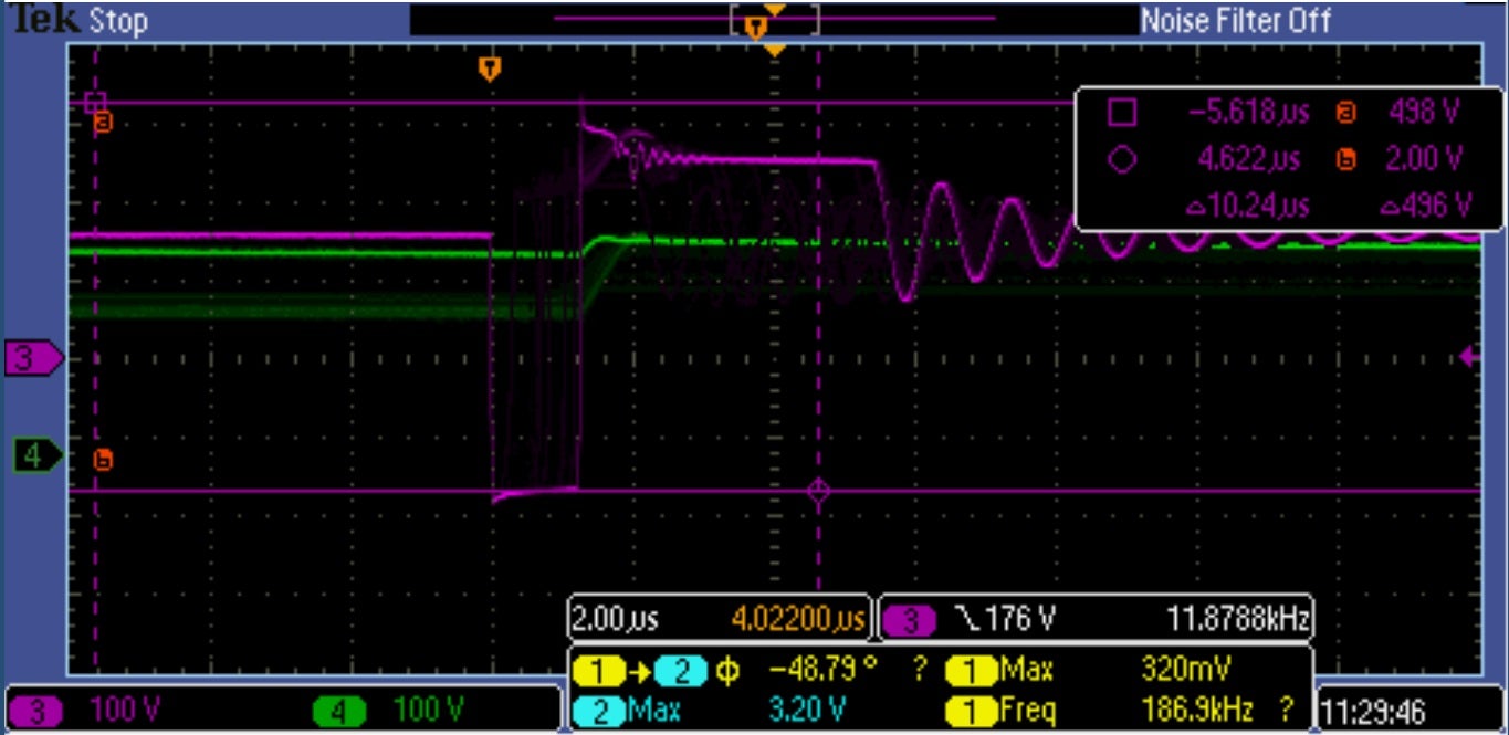
I think I solved the problem. Clamping circuit is not working with the transformer 1 and 2. I have attahched waveforms for 3 different situation with 2 different configurations. Green one is the voltage of the cathode of the TVS with respect to ground(source) and the pruple is the drain voltage with respect to gnd(source). When I use 180V TVS the 5.1ohm resistor immediately blows and the tvs is mostly on and the clamp does not work properly. First attachment shows that. When I changed tvs to 200V and increased resistor to 10 ohms the peak drain voltage soften and reduced dramatically. 2nd figure is taken at start-up and the 3rd one taken in steady state. Note that cathode voltage in figure 1 is taken in AC mode and 2,3 is taken in DC mode.
| Attachment | Size |
|---|---|
| snubber resistor 5.1ohm_180VTVS.jpg (167.67 KB) | 167.67 KB |
| 230VACIn_10ohm_200VTVS_Start_UP.jpg (146.74 KB) | 146.74 KB |
| 230VACIn_10ohm_200VTVS_SteadyState.jpg (163.63 KB) | 163.63 KB |
So it's all working now?
The slow rise of drain voltage after the sharp rise indicates that the snubber capacitor might be a bit small. Consider increasing the capacitance to make the clamping voltage ripple lower.
Your clamping voltage is still quite low. Consider increasing the snubber resistance (in parallel with cap) to increase the margin between the TVS clamping voltage and the RCD clamping voltage. This is what caused things to blow. The TVS isn't supposed to clamp 100% of the time. It's only for brief spikes.
transformer3 vds
| Attachment | Size |
|---|---|
| 230VACIn_5.1ohm_200VTVS_SteadyState_trans3.jpg (159.26 KB) | 159.26 KB |
transformer3 vds
| Attachment | Size |
|---|---|
| 230VACIn_5.1ohm_200VTVS_SteadyState_trans3.jpg (159.26 KB) | 159.26 KB |
transformer1 vds
| Attachment | Size |
|---|---|
| 230VACIn_10ohm_200VTVS_SteadyState_trans1.jpg (166.56 KB) | 166.56 KB |
Yes all are working now. I'll try your recommendations too and inform you. Thanks for your help.
I have tested with 2 transformers with different RC clamp values and attached the waveforms.
| Attachment | Size |
|---|---|
| 230VACIn_10ohm_200VTVS_6.9nF_33K_SteadyState_trans2.jpg (166.26 KB) | 166.26 KB |
| 230VACIn_10ohm_200VTVS_4.7nF_33K_SteadyState_trans3.jpg (160.87 KB) | 160.87 KB |
Hi,
When you increase the secondary turns, the reflected from secondary to primary reduces and which inturn reduces peack Vds across the primary MOSFET.
The device might be failing because of excess voltage on the Drain. As I said earlier you have to optimise your transformer design and snubber design.
Your design is single output design, ideally you should get very low leakage inductance. However I am not sure why leakage inductance is so high in your design. If you can send me your transformer construction document, I will be able to review and advice you.
Regards,
PI-NANO
Hi,
Do you know what eaxtly is the difference between the transformers?
Did you try sawpping the transformer from known good working board to the board that has problem. Does the problem go away with the transformer swapping?
Could you please verify the transformer winding polarity and terminations?
Did you measure all the transformer parameter measurements and how do they compare to each other?
Could you send us your schematics, and transformer construction document and PI Expert design file?
Regards,
PI-NANO