

Urgent help needed! Top249YN 10% fallout Bursting IC Shell
Hey Guy's
We have a Constant current driver 36/42V 1.05amp.
and about 10% of our drivers is failing after 10/14 days of use...
All these fails have the same issue a crack allong the full right side of the IC with burnmark asside them and at the right 2 pins...
This is a big issue for us could it be that this is because of heating and cooling causing some shells to show weaknesses and there by fail? Or could this be an other issue??
If anybody can help much appreciated!!
We love your components and we would love to keep working with them :D
But 10% fall out is to much :(
コメント
Is there anybody on the Forum active ...???
Hello renewh,
Thank you very much for using Power Integrations products and sorry for the late reply.
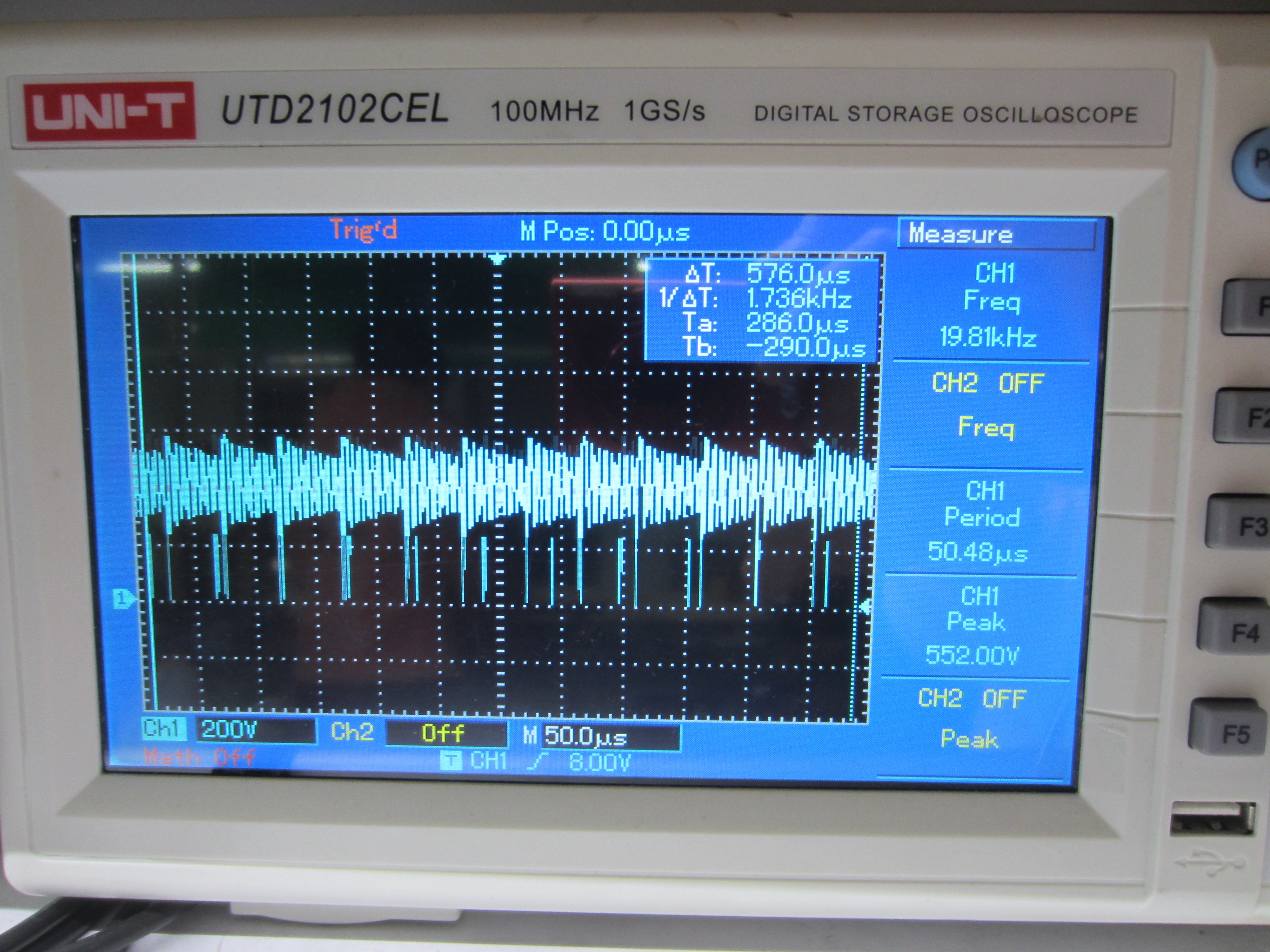
From the schematic you provided, it has a high input DC voltage for the top swicth which is 395V. did you ever check what is the maximum voltage across TOPswitch drain to source pin at the worst case condition. if you can send me some waveform of the Vds of the topswitch at high line, no load/full load condition, it will be very helpful to see how much margin we have for AMR of the drian voltage we have. i am wondering if the drain voltage is close to its AMR rating which is 700V. if we have no margin or little margin there, it is possible to damage the IC.
if you can tell me about the transformer turn ratios, it will also be very helpful.
Best Regards
Hi PI-YY,
Tnks for your respons.
We have done alle test and the highest spike we got in worstcase scenario was 624V..
I have the transformer document + images and movie of the diffrent wave forms but the files are really large.
Do you have a mail adres i could send it to with wetransfer?
With kind regards,
Rene
Hello renewh,
if the voltage is 624V, the device should be OK although not a lot of margin<10%. images should be good enough. i think you can upload the images through the web.
For the worst case scenario, what did you do for the worst case?
For the boost PFC stage, is there any chance we will get any overshoot under some transient period, like startup, load transient or line drop out?
Best Regards
Hi PI-YY,
I have forwarded your question to our engineer. I have waveform video and pictures if needed.
FOr the worstcase they took 300V input and 45V output.
| Attachment | サイズ |
|---|---|
| 220VAC no load (2).JPG (2.72 MB) | 2.72 MB |
| 220AC to 34VDC (3).JPG (3.08 MB) | 3.08 MB |
| 220VAC to 39VDC (2).JPG (3.03 MB) | 3.03 MB |
| 220VAC to 45VDC (1).JPG (3.05 MB) | 3.05 MB |
| 300VAC to 45VDC (1).JPG (2.82 MB) | 2.82 MB |
Hello renewh,
From the waveform you shared, I am wondering if your scope channel's filter is turned on. may I ask how much is your transformer leakage inductance. there should be a ringing after the MOSFET is turned off between the leakage inductance and Coss of the MOSFET which will give you a spike at your Vds. I didn't see that in your waveform, is this because of the leakage indcutance is really low. Can you confirm the filter in your scope is off when you measure the Vds.
you can take the waveform in below Top swicth DER for reference.
https://ac-dc.power.com/sites/default/files/PDFFiles/der218.pdf
Best Regards
Hi Pi-YY,
I just got feedback on your other question.
the PFC IC has its detecting logic on its output voltage, it checked the output every working period to ensure that it doesn't overshoot, so it's safe for transient states too
Can you work with this awnser or do i need to relay any other feedback on that
Hi PI-YY,
Here by the further respons from my engineer on your questions
[17-11-2016 7:29:10] the MOSFET of the PFC stage could bear 650V, while the top switch IC could bear 700V, if there's overshoot in the PFC stage's output, the MOSFET shall be broken first, but we only see the top switch broken not the MOSFET of PFC stage
[17-11-2016 7:30:29] we don't have protection at the PFC stage's output, but we don't think there is overshoot because the components in PFC stage are still good after top switch cracks
[17-11-2016 7:31:43] the leakage inductance of transformer is 22uH, it is very low so you don't see spike on the Vds waveform, our scope didn't have any filter on
Hello renewh,
Thank you for the confirmation with your engineer. For those boards which fail, did you have a change to check the board? is there anything else fail besides the Topswitch?
On the bench, is it possible to duplicate this failure like you mentioned cooling or heating? Another thing you can try is to check the Vds of the MOSFET during output short, both startup and steady state operation. if the voltage and current across the MOSFET is lower than its absolute maximum value. The part should not do any failure.
below is a reference design which is similar power level as yours. you can take that for reference.
https://ac-dc.power.com/sites/default/files/PDFFiles/der191.pdf
Best Regards




Anyone a idea :( were lightly in distress :(